SAN JOSE, Calif. ─ October 11, 2016 ─ One year after the debut of the industry’s first 200mm Fab Outlook report, SEMI has issued an October 2016 update, with the improved and expanded report forecasting 200mm fab trends out to 2020. This extensive report features trends from 2009 to 2020, showing how 200mm fab activities and capacity have changed worldwide. SEMI’s analysts updated information on almost 200 facilities, including new facilities and closures of existing facilities.
Examining 200mm capacity over the years, the highest level of 200mm capacity was recorded in 2007 and the lowest following this peak in 2009 (see figure). The capacity decline from 2007 to 2009 is driven by the 2008/2009 global financial crisis, which caused the closure of many facilities, and to the transition of memory and MPU fabrication to 300mm fabs from 200mm.
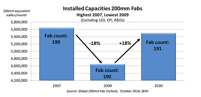
Since 2009, installed 200mm fab capacity has increased, and by 2020, 200mm capacity is expected to reach 5.5 million wafers per month (wpm), though still less than the 2007 peak. According to SEMI’s data, by 2019, installed capacity will reach close to 5.38 million wpm, almost as high as capacity in 2006. From 2015 to 2020, 200mm facilities are forecast to add 618,000 wpm net capacity. This increase is a combination of fabs adding capacity and fabs losing capacity.
Two applications account for the growing demand for 200mm: mobile devices and IoT. Rising fab capacity from 2015 to 2020 will be driven by MEMS devices, Power, Foundry and Analog. By region, the greatest increases in capacity are expected to be in China, Southeast Asia, Americas, and Taiwan. Another trend is also observed: 200mm fabs are increasing the capacity to provide process capability below 120nm. Higher capacity does not mean more fabs, but fewer, larger fabs. In fact, the number of fabs in 2020 is almost the same as the count seen in 2009. So 2020 capacity heads toward industry highs while in comparison 2009 had the lowest levels off the 2007 peak.
The Global 200mm Fab Outlook to 2020, published by SEMI in October 2016, includes two files: a 92-page pdf file featuring trend charts, tables and summaries and an Excel file covering 2009 to 2020 detailing on quarterly basis and fab-by-fab developments. For more information about SEMI, visit www.semi.org and follow SEMI on LinkedIn and Twitter.
About SEMI
SEMI® connects more than 2,000 member companies and more than a quarter-million professionals worldwide to advance the science and business of electronics manufacturing. SEMI members are responsible for the innovations in materials, design, equipment, software, and services that enable smarter, faster, more powerful, and more affordable electronic products. Since 1970, SEMI has built connections that have helped its members grow, create new markets, and address common industry challenges together. SEMI maintains offices in Bangalore, Beijing, Berlin, Brussels, Grenoble, Hsinchu, Moscow, San Jose, Seoul, Shanghai, Singapore, Tokyo, and Washington, D.C. For more information about SEMI, visit www.semi.org and follow SEMI on LinkedIn and Twitter.
Association Contact
Deborah Geiger
SEMI Headquarters
Phone: +1.408.943.7988
Email: dgeiger@semi.org
# # #