A Bright or Bleak Future: Semiconductor Fabs in China
By Samuel Ni
Until up to the end of 2004, the regional managers for the semiconductor fab equipment vendors very much enjoyed the strong growth in the China market. The sudden slowing down in capital expenditures by major fabs in 2005 showed that China was not immune from semiconductor industry cycles. The almost 50 percent decline in overall capital expenditures by fabs and foundries in 2005 dampened immediate prospects for growth in China and reminded industry observers that investment plans need to be based on sound business analysis.
With the slowdown, business became a little more bit complicated in China as some announced fab projects experienced difficulty raising funds or securing a technology partnership. As a result, some fab projects may be permanently delayed and forever be an unfulfilled wish by their backers. A review of the various fab projects announced from 2001 and 2004, shows that close to 50 percent of the announced fab projects were delayed, suspended, or simply cancelled. For insiders and longtime observers of China’s semiconductor industry, nothing is unique about these failed projects when accounting for logical business considerations. For some outsiders, however, serious questions may be raised about the future of China’s fab industry: is it bright or is it bleak?
The reality of the China market to date is that some projects indeed did not get off the ground; though in no means does this mean that half of the fabs will fail there in the future. Numerous 200 mm and 300 mm fabs are currently being planned, constructed, equipped and ramped for production in China. Just in the last eight months, several new fab projects have been announced.
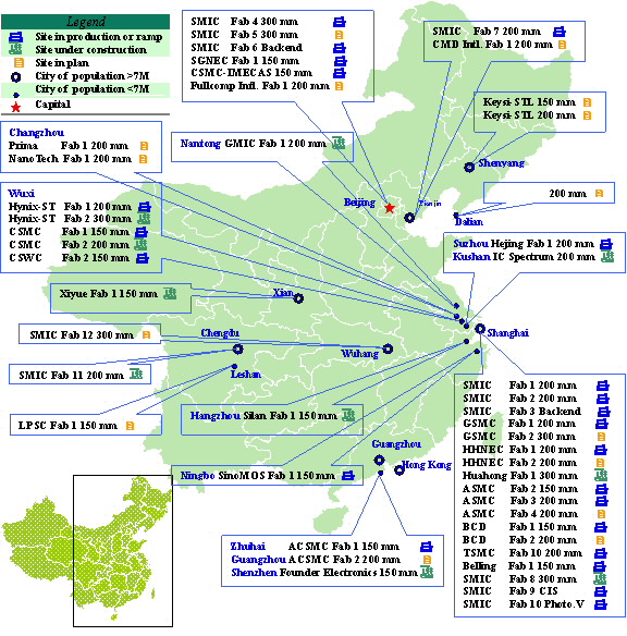
What has changed is that some of the previously exuberant expectations about the China market have dissipated. New projects are moving forward and government support is shifting to state-owned or state-controlled semiconductor manufacturers such as Huahong Semiconductor. Meanwhile, local bank credits for fab projects are not disappearing, but will be more difficult to secure. Fab projects that bring advanced technology or significant foreign direct investment will be relatively easier to get financing. The map highlights current fabs and new projects in China.
Locations of Major 150 mm–300 mm Established and Future IC Fabs in China
Over the next few years, leading semiconductor manufacturers in China will be moderate in terms of capital expenditures and will make greater use of used equipment for 200 mm fabs. The future for new fab projects by established semiconductor manufacturers, like the Hynix-ST Microelectronics joint-venture, are more promising than projects by new “green field” entrants. Spending for new 300 mm wafer fab equipment will dominate in the coming years with entry-level process technology at the 0.13 µm node. New 300 mm equipment is expected to account for 70 percent of $2 billion in total new fab equipment spending forecasted for 2008. The fab materials market is expected to grow to $1.4 billion by 2008, almost three times above 2005 spending levels.
As China is further assimilated into the global economy, its semiconductor industry will continue the rapid pace of development that the country has experienced since 2000. The 2005 slowdown has shown that China is not exempt from the sometimes volatile swings in customer demand felt by the worldwide semiconductor industry. Yet, China continues to invest in new capacity and in new fabs. Industry observers may question China’s continued investments even when capacity utilization is low or the market lacks a major driver, but China’s national growth strategy calls for more fabs and greater capacity.
All of the information in this article was derived from a recently completed market research study, China Semiconductor Wafer Fab and Foundry Outlook, produced by SEMI.
The report contains information on trends related to fab and foundry investments in China and is based on over 60 in--person interviews with semiconductor manufacturers, equipment and material suppliers, fab construction companies, government officials and local industry associations.
TO ORDER YOUR COPY of China Semiconductor Wafer Fab and Foundry Outlook please call SEMI Global Sales & Services at 408.943.6901. You can also visit www.semi.org and select STORE from the horizontal menu to find order information for this report.
About the Author:
Samuel Ni is a senior market analyst of SEMI China and the co-author of SEMI’s report of “China Semiconductor Wafer Fab and Foundry Outlook”. Mr. Ni can be contacted by email at [email protected]