June 30, 2021 - June 30, 2022
View this Master Class On Demand! Learn why and how new packaging paradigms like chiplets and dielets are impacting the world of flexible hybrid electronics (FHE) from one of the industry's foremost experts, Dr. Subramanian Iyer of UCLA. The course explores how these packages are packing such a punch and enabling advanced performance in a much smaller and flexible footprint.
Time
10:00 am - 12:00 pm
Location
On-Demand, Online,
United States
OVERVIEW
In the last few years, electronics packaging has rightfully emerged from the shadows of CMOS scaling to make a significant impact in high performance and mobile appliance computing.
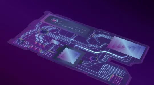
In this course, we reviewed the key developments in this paradigm change and the implications these have on Flexible Hybrid Electronics especially the use of bare dielets, fine pitch interconnects and novel substrate materials.
The area of Flexible Hybrid Electronics (FHE) has also developed and is making a significant impact in the area of medical and wellness electronics. The first generation of these devices have, for most part, adapted Printed Circuit Board (PCB) technology by using thinner PCBs and assembling either thinned or thin packaged “older” generation of chips on to these platforms, typically with coarse printed wiring to connect a small number of such chips.
This approach, while immensely useful to get the field going, needs to adapt and borrow from the both silicon and advanced packaging technology trends, so that we can advance this trend to the next level. The key paradigm challenges ahead are: scaling FHE in general – this includes the adoption of dielet (chiplet) technology in more advanced CMOS nodes including edge-AI, higher performance interconnects, flexible high-density energy storage, wireless communication and advanced ergonomics and all of these at lower cost and higher reliability.
This talk addresses the challenges and outline a possible technology roadmap to achieve these goals in the next few years.
Featured Speaker Biography: Subramanian S. Iyer (Subu) is Distinguished Professor and holds the Charles P. Reames Endowed Chair in the Electrical Engineering Department and a joint appointment in the Materials Science and Engineering Department at the University of California at Los Angeles. He is Director of the Center for Heterogeneous Integration and Performance Scaling (CHIPS). Prior to that he was an IBM Fellow. His key technical contributions have been the development of the world’s first SiGe base HBT, Salicide, electrical fuses, embedded DRAM and 45nm technology node used to make the first generation of truly low power portable devices as well as the first commercial interposer and 3D integrated products. He also was among the first to commercialize bonded SOI for CMOS applications through a start-up called SiBond LLC.
More recently, he has been exploring new packaging paradigms and device innovations that they may enable wafer-scale architectures, in-memory analog compute and medical engineering applications. He has published over 300 papers and holds over 75 patents. He has received several outstanding technical achievements and corporate awards at IBM. He is an IEEE Fellow, an APS Fellow, an iMAPS Fellow and a Distinguished Lecturer of the IEEE EDS and EPS and a member of the Board of Governors of IEEE EPS. He is also a Fellow of the National Academy of Inventors. He is a Distinguished Alumnus of IIT Bombay and received the IEEE Daniel Noble Medal for emerging technologies in 2012 and the 2020 iMAPS Daniel C. Hughes Jr Memorial award.
SEMI Members: $49
Use your corporate email address during log in to be recognized as a SEMI Member.
Non-Members: $99
Students: Free
Contact Gity Samadi (gsamadi@semi.org) with a picture of your student ID to receive your discount code.