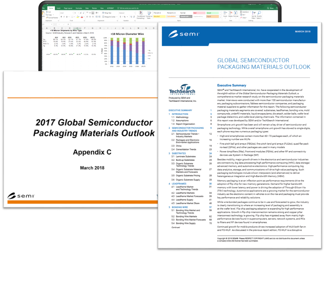
Global Semiconductor Packaging Materials Outlook (2017 to 2021)
A comprehensive study that examines the semiconductor packaging materials markets with forecast through 2021
Publication Date: 4.17.2018
Principal Analysts: Dr. Dan Tracy of SEMI and E. Jan Vardaman of TechSearch Inc.
Number of pages: 120+
Format: Microsoft® Excel® (.xls) and PowerPoint (.ppt) and Adobe® .pdf (includes three files)
Overview
|
Global Semiconductor Packaging Materials Outlook is a comprehensive market research study that examines semiconductor packaging technology trends and their impact on the packaging materials markets. Packaging materials markets are quantified; new opportunities are highlighted for advanced technology nodes and emerging package form factors, and forecasts through 2021 are presented. Global Semiconductor Packaging Materials Outlook is an essential business tool for anyone interested in the plastic packaging materials arena. Packaging materials directly affect the performance, reliability, and cost of semiconductors, and offer significant improvement potential.
|
 |
![]() Request a Sample ( 2018 Sample includes 2015 Report Executive Summary)
Request a Sample ( 2018 Sample includes 2015 Report Executive Summary)
Product Information
| Features | |
|
|
Benefits
- Gain insight to worldwide packaging material technology trends, market size, and market forecast
- Understand key package offerings and technologies
- Use benchmark data to validate business opportunities and assumptions
- Improve business analysis and empower your market research with verified, validated, and credible data
Purchase Global Semiconductor Packaging Materials Outlook
| Product ID# | Product Description |
Member* |
Non-Member | |
| 3566 | Global Semiconductor Packaging Materials Outlook (with Forecast to 2021) -Single-user | $4,500 | $5,100 | Buy Now |
| 3567 | Global Semiconductor Packaging Materials Outlook (with Forecast to 2021) - Multi-user | $12,500 | $15,000 |
*Pricing does not apply to Individual Members.
For product related inquiries or questions regarding Enterprise pricing, please email mktstats@semi.org or call 1.877.746.7788.
Other Related Reports
SEMI China Semiconductor Packaging Market Outlook, 2018 Edition
Worldwide OSAT Manufacturing Site Database
Table of Contents
EXECUTIVE SUMMARY
1 INTRODUCTION
1.1 Methodology
1.2 Assumptions
1.3 Report Organization
2 SEMICONDUCTOR PACKAGING AND INDUSTRY TRENDS
2.1 Semiconductor Trends - Industry Markets
2.2 Semiconductor Trends - Regional and Market Issues
2.3 Packaging Materials Needs – Customer Input
2.4 Packages and Electronic End-market Applications
3 SUBSTRATES
3.1 Laminate Substrates
3.2 Build-up Substrates
3.3 Organic Substrate Technology Trends
3.4 Organic Substrate Material Markets and Forecasts
3.5 Organic Substrate Pricing
3.6 Organic Substrate Supply
3.7 Flex Circuit/Tape Substrates
4 LEADFRAMES
4.1 Leadframe Market and Technology Trends
4.2 Leadframe Markets
4.3 Leadframe Market Forecasts
4.4 Leadframe Supply
5 BONDING WIRE
5.1 Bonding Wire Market and Technology Trends
5.2 Bonding Wire Markets
5.3 Bonding Wire Pricing
5.4 Bonding Wire Market Forecasts
5.5 Bonding Wire Supply
6 MOLD COMPOUNDS
6.1 Mold Compound Technology Trends
6.2 Mold Compound Markets
6.3 Mold Compound Market Forecasts
6.4 Mold Compound Supply
7 UNDERFILL MATERIALS
7.1 Capillary Underfill (CUF)
7.2 Molded Underfill (MUF)
7.3 Non-conductive Paste (NCP)
7.4 Non-conductive Film (NCF)
7.5 Underfill Technology Trends
7.6 Underfill Material Market
7.7 Underfill for Packages
7.8 Underfill
8 LIQUID ENCAPSULANTS
8.1 Liquid Encapsulant Technology Trends
8.2 Liquid Encapsulant Markets
8.3 Liquid Encapsulant Market Forecasts
8.4 Liquid Encapsulant Supply
9 DIE ATTACH MATERIALS
9.1 Die Attach Technology Trends
9.2 Die Attach Markets
9.3 Die Attach Market Forecasts
9.4 Die Attach Supply
10 SOLDER BALLS
10.1 Solder Ball Material Technology Trends
10.2 Solder Ball Market and Forecast
10.3 Solder Ball Supply
11 WATER LEVEL PACKAGE
11.1 Wafer Level Package Dielectrics Technology Trends
11.2 Wafer Level Package Dielectrics Market and Forecast
11.3 Wafer Level Package Dielectrics Supply
12 PLATING CHEMICALS
12.1 Plating ChemicalsTechnology Trends
12.2 Plating Chemicals Material Development
12.3 Plating Chemicals Market and Forecast
12.4 Plating Chemicals Material Supply
13 SUMMARY AND CONCLUSIONS
13.1 Acknowledgements
14 APPENDICES
Purchase Global Semiconductor Packaging Materials Outlook - Available Now!
| Product ID# | Product Description |
Member* |
Non-Member | |
| 3566 | Global Semiconductor Packaging Materials Outlook (with Forecast to 2021) -Single-user | $5,000 | $6,000 |  |
| 3567 | Global Semiconductor Packaging Materials Outlook (with Forecast to 2021) - Multi-user | $12,500 | $15,000 | |
*Pricing does not apply to Individual Members.
For product related inquiries or questions regarding Enterprise pricing, please email mktstats@semi.org or call 1.877.746.7788.
Methodology
In-person interviews with material suppliers, packaging subcontractors and semiconductor manufacturers around the world are the sources of information for this study. Market size information is developed through primary research and modeling. Five-year market forecasts are developed based on different scenarios of new technology penetration and market growth.
Other Reports
Worldwide OSAT Manufacturing Site Database
Material Market Data Subscription (MMDS)
World Fab Forecast
World Fab Watch