会社概要
東芝ナノアナリシス株式会社は、2002年8月に株式会社東芝の
Company Info
Toshiba Nanoanalysis Corporation was established in August 2002 inheriting the expertise and knowledge of analysis and evaluation accumulated in Toshiba Corporation. We offer various analytical services for nanostructure, surface, thin film, semiconductor, FPD, electronic components, reliability evaluation, failure analysis, clean room assessment, inorganic and organic chemistry analysis and analysis for pharmaceutical and medical treatment.
Highlights
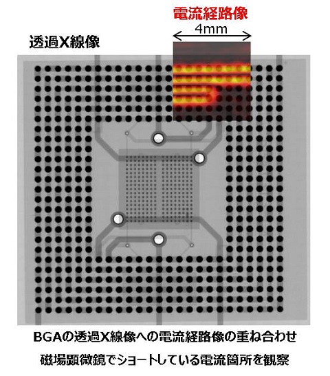
The number of IoT apparatus in which many electronic components such as sensors, IC, memories, resistors and capacitors are mounted, are increasing exponentially. High reliability is required for those devices because they are used in various environments regardless of indoor and outdoor. We support those developments of IoT apparatus based on various technologies such as fault localization by non-destructive observation using combination of magnetic field and X-ray microscope capable of visualization of electric current paths and observation of light elements, and 3D physical analysis using FIB-SEM/EDS with sophisticated sample preparation.
Products/Services
A magnetic field microscope is a technology which acquires the magnetic field distribution generated by electrical current, performs mathematical processing, and visualizes the current pathways without sample destruction. The magnet field microscope detects unusual current pathway, and then 3D X-ray microscope pinpoints the fault location in detail. Furthermore, the information on materials is acquirable in 3D by reconstructing the image acquired by repeated FIB processing, SEM observation, and EDS analysis using software. The three-dimensional grasp of a defect or a void is connected with investigation of the cause of fault.
1