3D Packaging and Integration標準化技術委員会設立の紹介
日本地区3D Packaging and Integration技術委員会共同委員長
2017年7月14日に開催された、国際スタンダード委員会会議にて、従来のPackaging and Assemblyグローバル技術委員会と3DS-IC グローバル技術委員会が統合して3D Packaging and Integrationグローバル技術委員会となることが承認され、北米、台湾及び日本の各地区で始動しました。
1.二つのグローバル技術委員会統合の背景
エレクトロニクス産業を取りまく環境は劇的に変化しています。主な四つの要因として挙げられるのは、1)Internet of Things(IoT)、2)データ、ロジックやアプリケーションのクラウドへの移行、3)一般消費者向けデータ生成とアクセスの増加、および4)パッケージ技術による形を変えたムーアの法則の継続などがあります。
新しいアーキテクチャとプラットフォームが登場し、クラウドインフラストラクチャに移行することで、画像集約型アプリケーションの大幅な需要増やデータ分析集約型バーチャルリアリティ、さらに人工知能などの様々なアプリケーションに適応することができるようになってきました。これら新しく創造された市場は、グローバルネットワークとそれに接続されているすべての変化を求め続けています。パッケージング技術の進化が、より高い性能、より低い消費電力、帯域幅の物理密度の増加とレイテンシーの減少を、コストの上昇なしに実現することができることを示してきた。
事実、Emerging Packaging技術が多く生まれてきました。例えば、ウェーハレベルパッケージ技術、2.5D や3D Integration、SiP (System in Package)およびHeterogeneous Integrationなどは製品の小型化の継続を可能にする主な要素となっています。歴史的にみても、パッケージ技術はICの機能の向上と物理的サイズの小型化のために、寸法および電気・熱的な対応を十分に担ってきています。
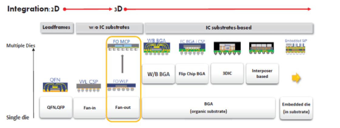
図1 パッケージ技術の推移(出典:Yole Development)
図1に最近の主なパッケージ体系を示しました。リードフレームを使ったパッケージとしてQFNやQFPなどがあり、有機基板を使ったBGAやFlip Chip BGAパッケージ、いくつかのチップを積層した3D-IC パッケージなどがあります。また、有機基板を使わないWafer Level Package (Fan-inタイプ、Fan-outタイプ)さらに半導体チップやパッケージおよび受動部品などをプリント配線板に埋め込む部品内蔵技術も用いられています。
2.新たなグローバル技術委員会の必要性
SEMI標準化技術委員会では、従来Packaging and Assemblyグローバル技術委員会で、レガシーパッケージの材料技術、検査・試験技術や梱包関連技術の標準化を行ってきました。また、3DS-IC グローバル技術委員会では、ウェハやチップを三次元に積層する際の関連技術、例えばTSV(Through Silicon Via) 技術やウェハ薄化に関する標準化を行ってきました。
近年のパッケージ技術の進化と多様化により、パッケージの形態や適用される技術・材料・装置だけでは必要とされる標準規格が分類できない状況になっており、Packaging and Assemblyグローバル技術委員会と3DS-IC グローバル技術委員会での棲み分けが困難になってきています。そこで、この二つのグローバル技術委員会を統合する提案が、SEMICON West 2017開催期間中の7月14日の国際スタンダード委員会(International Standards Committee)会議で承認され、時流に合った新たな委員会、3D Packaging and Integrationグローバル技術委員会が、北米、台湾及び日本の各地区で始動しました。
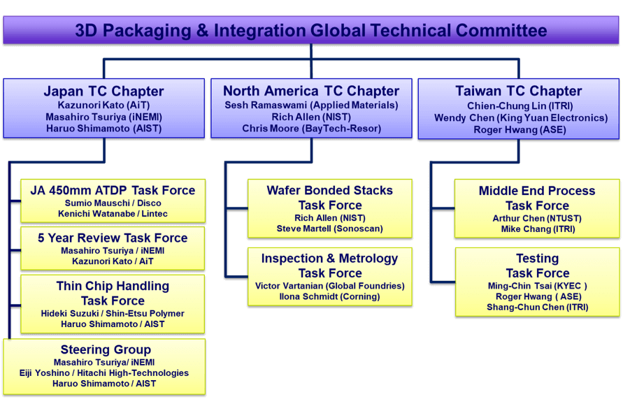
図2 新たなグローバル技術委員会(Global Technical Committee)の組織
3.3D Packaging and Integrationグローバル技術委員会の設立目的・役割、活動範囲
この3D Packaging and Integration グローバル技術委員会の活動範囲は、これまでの二つの委員会が担っていた範囲に加え、FO-WLP(Fan-out Wafer Level Package), PLP(Panel Level Package) や部品内蔵技術も視野に入れています。下記に承認されたCharter/Scopeを記します。
① Charter
To explore, evaluate, discuss, and create consensus-based specifications, guidelines, test methods, and practices that, through voluntary compliance, will:
- include the materials, piece parts, and interconnection schemes, and unique packaging assemblies that provide for the communication link between the semiconductor chip and the next level of integration, either single- or multi-chip configurations. It relates to the technologies for heterogeneous and other multi-chip packaging such as Fan-out/Fan-in Wafer Level Packaging, Panel Level Packaging, Three-Dimensional Stacking IC, device embedded packaging, flexible electronics technology
- promote mutual understanding and improved communication between users and suppliers, equipment, automation systems, devices, and services
- enhance the manufacturing efficiency, capability and shorten time-to-market and reduce manufacturing cost
② Scope :
- The 3D Packaging and Integration Committee develops standards for semiconductor devices, including processed wafers, chips, or multi-chip configurations to the next level of integration, either in single- or multi-chip configurations
- materials needed for 3D applications, including prime silicon and glass wafers, temporary and permanent bonding material, specifications needed for processed wafers and/or chips to enter an integration step, etc.
- the materials related to the elements of, interconnection schemes, and unique packaging assemblies that provide for the communication link between device and packaging
- the technologies for heterogeneous and other multi-chip packaging such as Fan-out/Fan-in Wafer Level Packaging, Panel Level Packaging, Three-Dimensional Stacking IC, device embedded packaging, and flexible electronics technology
- metrologies to support these 3D integration and packaging technologies
半導体やエレクトロニクス製品がこれまで以上に多くの分野に素早く普及・活用されるようにするためには、標準化活動は非常に重要であり、新しくできた委員会が果す役割も大きいものとなります。多くの方の参画を期待いたします。
3D Packaging and Integration標準化活動にご参加を希望される場合には、以下にお問合せください。
SEMIジャパン スタンダード & EHS 部 柳澤智栄
03-3222-6018(部代表) / cyanagisawa@semi.org