Monozukuri of Rome, Italy, one of the newest members to join the ESD Alliance, a SEMI Technology Community, is out to conquer 2.5D and 3D design challenges for next-generation electronic products by delivering innovative, groundbreaking EDA software solutions and methodologies. The company’s technology redefines the co-design of heterogeneous microelectronic systems by providing an improved level of automation in three-dimensional interconnect optimization.
Anna Fontanelli, Monozukuri’s founder and CEO, is an expert in deep-submicron silicon technology and design tools. She shared her perspectives on the state of Moore’s Law and challenges surrounding 2.5D integration, 3D chip stacking and advanced packaging, as well as the chip design industry’s startup environment.
Smith: Why is there so much interest in chiplets?
 Fontanelli: Candidly, chiplet development and advanced packaging will determine the future of the semiconductor industry. Moore’s Law, if it really was ever a law, has hit the wall of physics. You can fool physics some of the time, but long-term, it is a fool’s errand.
Sure, we’ll see new exotic materials, even creatively reconfigured transistors. The fact is that economically, and technically, chiplet and package development create the pathway to continuing the pace of innovation which, of course, was the intention of Gordon Moore when he postulated his doubling-performance hypothesis.
Smith: What is driving the need for advanced packaging?
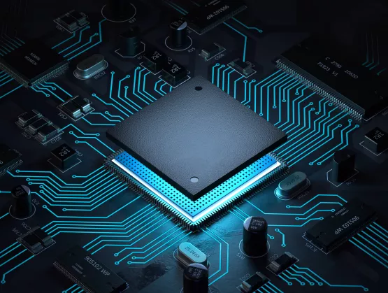
Fontanelli: New silicon applications like graphics processing units (GPUs), tensor processing units (TPUs), and artificial intelligence/machine learning (AI/ML) chips are reaching the limit of the maximum reticle sizes and require huge amounts of closely integrated components. The only way these high-end systems can achieve their power and performance goals is through the intimate integration of multiple dice on an interposer substrate (2.5D-IC), or by stacking dice directly on top of each other (3D-IC and High-Bandwidth Memory (HBM).
Strong economic reasons are driving the deconstruction of systems on chips (SoCs) into a heterogeneous collection of smaller die that then need to be integrated on a die-to-die substrate. A number of key factors need to be considered on an advanced package design, such as thermal and mechanical effects as well as electrical performance including I/O planning, power consumption and performance.
Smith: With all of these new ways of speeding the pace of innovation, where does Monozukuri fit into these trends?
Fontanelli: I really think we started Monozukuri at the right time. You’re right, the confluence of a number of challenges is continuing the industry’s pace of innovation. Ultimately, there is need to look at the problem from a holistic, systems perspective. That’s easier said than done, given the complexity of designing at today’s advanced technology processes.
 What is required is the simultaneous, integrated design of both chiplet-based systems and packaging. The promise of a tool that integrates I/O planning, management and optimization for all 3D-IC and chiplet-based systems has been bandied about for a number of years. It needs to enable designers to quickly and easily assemble complete cross-domain systems (ICs and package), drive pin assignment, and optimize through a rule-based methodology.
One product integrates single or multiple high-pin count chiplets, ASICs, and silicon interposers into a wide variety of package configurations, and supports wire-bond, flip-chip or mixed assembly designs. It offers drag-and-drop functionality to create the system directly in a graphic system view. With a common methodology, the system architect controls the design from either an IC-centric or package-centric perspective during early planning, prototyping, or detailed implementation.
Smith: That sounds like a very complex challenge.
Fontanelli: It is and may be solved with one-step systems optimization. A 3D-aware cross-hierarchical pathfinding algorithm and methodology can deliver one-step interconnect optimization throughout the entire system hierarchy, from level 0 (PCB) to level n, supporting an unlimited number of hierarchy levels. Automated underlying algorithms can reduce signal congestion and shorten the interconnections, providing significant benefits for pin assignment optimization and wire lengths/crossovers reduction that results in an extremely efficient use of routing resources.
Smith: How is the semiconductor industry’s startup environment? Is there a support network for entrepreneurs?
Fontanelli: In Europe, it’s interesting. We don’t have the robust venture capital infrastructure that you see in the U.S. We do have an active EU/state-sponsored infrastructure embodied in Horizon 2020 and, more recently, Horizon Europe 2021-2027. These initiatives facilitate the creation of multi-disciplinary and multi-partner consortiums that support the electronic ecosystem through funding innovative research projects. Horizon 2020 funded Monozukuri’s underlying technology. Going forward, we’ll probably leverage Horizon Europe for microelectronic and photonics design integration, and projects to meet the thermal and power challenges.
About Anna Fontanelli
Anna Fontanelli has more than 25 years of expertise in managing complex R&D organizations/programs to give birth to innovative EDA technologies. Fontanelli is an expert in IC/package co-design and led Monozukuri in the launch of GENIO, bringing a holistic design environment for 2D, 2.5D and 3D multi-component systems.