The global chip shortages together with the growing trends of electrification and digitalization have heightened awareness of the world’s reliance on semiconductors. A recent report by global management consultancy McKinsey & Company1 points to the increasing pace of digital transformation, predicting a decade of growth leading to a $1 trillion semiconductor industry by 2030.
Semiconductor Market Growth to 2030
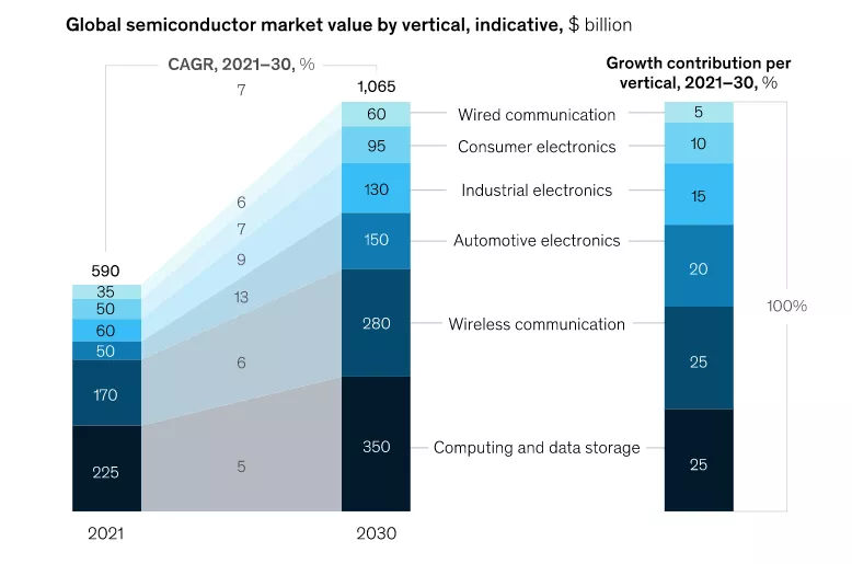
Source: McKinsey & Company
The semiconductors being developed to address future demand will be more powerful, more sophisticated and integrate more functionality than ever before. While debate continues about how long Moore’s Law can strictly be applied, it has served the industry well for almost 60 years and has continued relevance as designers drive the capabilities of their chips to ever-new heights. Turning designs into reality requires transformative fabrication processes with hundreds of sequential steps that are expected to deliver high yields with maximum productivity and minimum downtime, even as complexity and power demands rise.
Precisely controlled, reliable high-voltage power plays a critical role in meeting these expectations.
Various Power Requirements for Semiconductor Manufacturing Processes
The main power supplies and associated technologies required to support today’s semiconductor manufacturing processes.
For etch and deposition, the days of the simple switch mode power supply (SMPS) are gone as the techniques that create the high aspect ratio (HAR) circuits in the latest semiconductors have become more complex. Now multiple radio frequency (RF) power supplies generate and control the plasma inside the process chamber while etching patterns onto wafers. Combining these power supplies with impedance matching networks enables manufacturers to maximize throughput while keeping process power as low as possible by responding nearly instantaneously to changes in the etch or deposition process steps as power is transferred to the plasma.
Modern ion implant processes also demand a combination of power supplies and matching networks. Here, processes may use power supplies with output voltages in the tens of kV for precision electron and ion beam acceleration, scanning and control as well as high-voltage pulsed DC power supplies that minimize arcing, enhance deposition rate, improve film flatness and packing density. In addition, high-voltage power amplifiers support ion beam steering.

Electrostatic voltmeters (ESVMs) have become critical elements in wafer control during fabrication. Measuring electrostatics poses special problems because electrostatic systems are generally characterized by high resistances and small amounts of electrical charge that prevent the use of conventional electronic instrumentation. ESVMs provide highly accurate non-contact surface electrostatic voltage measurements during etch, deposition and ion implantation and are also used to optimize the force applied in the electrostatic chucks (ESCs) that clamp the wafer, during handling and processing.
When it comes to inspecting wafers, the challenge is to measure the dimensions of the fine patterns without impacting throughput. With today’s technologies, this requires rapid processing of high aspect ratio features and complex three-dimensional architectures with down to sub-nanometer resolutions. In turn, this demands high-voltage power and control solutions that ensure stable and accurate power delivery.
Another critical power requirement for semiconductor fabrication comes from the need to keep the CVD, PECVD and PEALD plasma chambers as clean as possible during operation to minimize or eliminate major chamber cleans that result in process downtime. This inline cleaning is typically achieved with a remote plasma source (RPS) that uses an RF-generated plasma to dissociate gases, such as NF3, to clean the chamber.
Technologies for Today’s Process Power Requirements
The need for ever-more precise process control and more targeted and efficient power delivery is driving significant process power innovation.
In the case of RF power, for example, the latest power supplies and match networks respond nearly instantaneously to changes in the etch or deposition process steps as power is transferred to the plasma. One recent innovation is the asymmetric bias waveform generator that applies metrology and waveform control to deliver the precise bias plasma performance needed for sensitive feature formation in HAR dielectric structures at high speeds.
The latest matching networks equipped with microprocessor-controlled stepper motor drives and advanced tuning algorithms further support optimized delivery of RF power by speeding tuning and match response times. Some of these networks integrate RF sensors to provide real-time analysis of process power and impedance, enabling operators to quickly identify and reduce process variability.

For ion implantation and ion beam applications, operators can choose from a variety of IGBT-based AC-to-high-voltage DC (AC to HVDC) power supplies that ensure efficient, reliable operation over the full operating range. Rack-mount and module-based E-Beam power supplies designed for the scanning electron microscopes (SEMs) deployed in semiconductor inspection increasingly offer built-in flexibility to accommodate various Schottky emission electron gun configurations as well as digital control that enables operational and diagnostic capabilities through intuitive GUIs.
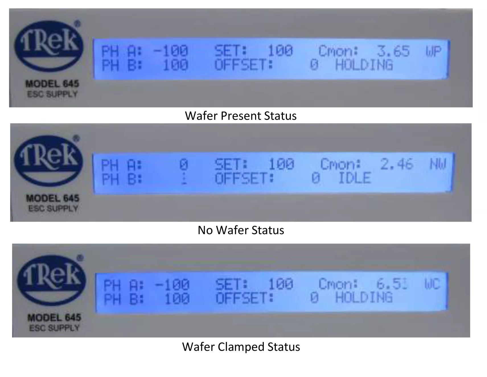
Power supply solutions for electrostatic chucks are also evolving, with the ESC supplies that provide the best performance now largely based on high-voltage amplifier technology. Because ESCs are predominately capacitive in nature, a HV amplifier provides the highest level of performance when clamping and de-clamping wafers. The latest amplifiers provide 4-quadrant operation, can supply and sink current independently of output voltage and provide control parameters such as over-current, wafer-present and wafer-clamped thresholds as well as clamp voltage, offset voltage and internal or external amplitude/offset control.
Real-time Wafer Status Information Displayed on High-voltage ESC Amplifier
The High-Voltage Journey
Reliable, high-voltage power is essential for semiconductor fabrication in areas such as ion implantation, deposition, etching, e-beam lithography, process metrology and inspection, as well as semiconductor testing. As we transition to smaller nodes, advanced wide bandgap (WBG) and 3D technologies, precise control of this power becomes more important. Power supply manufacturers should not only address today’s requirements but anticipate future needs and provide operators with the flexible platforms that will allow them to address future challenges.
Ray Morgan is Advanced Energy’s Vice President and General Manager of High-Voltage Systems.