Three-dimensional integrated circuits (3D-ICs) are revolutionizing the semiconductor industry. Manufactured by stacking and interconnecting dies so they perform as a single device, 3D-ICs deliver more capabilities by offering higher performance and bandwidth — while also reducing power consumption, package size and costs.
However, 3D-ICs present tough design challenges to engineers. Significantly larger than a single-chip system on a chip (SoC), these assemblies have more components, more integration points and longer interconnects, that translate to new risks for high-frequency signal failure, reliability, and other performance issues such as thermal buildup.
As the lines between silicon and system continue to blur, engineers must conduct concurrent, multivariate analysis to assess every possible failure mode ― not only at the component level, but also across the entire 3D-IC assembly ― a technical obstacle for many development teams accustomed to applying a series of single-physics engineering simulation tools in a sequential approach.
3D-ICs are assembled in a complex package using a serial analysis approach that doesn’t take into account system-level interactions, as well as the many thousands of bump connection points where something can go wrong. By contrast, concurrent, multivariate simulation and analysis takes into account all physics simultaneously from the earliest prototyping stages of design.
 Most semiconductor development teams not only lack the technical tools to perform this complex simulation and analysis, but they also face cultural obstacles as they undertake system-level analysis. Diverse teams working with disparate tools simply aren’t equipped to perform seamless handoffs and collaborate effectively on a complex 3D IC design from an early stage. Instead, they scramble to address system-level issues later when launch delays are likely, the cost of rework is high and their positive contributions to the design are diminished.
The Value of a True Multiphysics, Multivariate Approach
As market demand for 3D-ICs increases, semiconductor development teams need a single simulation platform that enables simultaneous multiphysics analysis — including power integrity, reliability, electromagnetics (EM), thermal, computational fluid dynamics (CFD) and mechanical studies ― across the entire assembly.
A unified simulation platform that brings together best-in-class solutions for every physics enables semiconductor engineers to collaborate across functions, seamlessly hand off analysis tasks between engines, and partner to optimize 3D-IC designs across every performance parameter. Costly surprises from signal integrity to thermal conductivity and structural strength are far less likely when the team reaches physical assembly to help ensure on-time, cost-effective product launches.

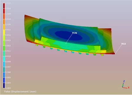
An example of simultaneous multivariate analysis of a chip stack showing both thermal gradients and mechanical stress/warpage of the package at an early prototyping stage.
By contrast, applying multiple physics sequentially can lead to ongoing and expensive setbacks. For example, as one team resolves signal integrity issues, another team could discover that timing failures or thermal risks have arisen. It’s not only back to the drawing board, but back to a series of time- and resource-intensive handoffs across disconnected simulation and analysis tools, as well as across functional boundaries.
The Importance of Considering Novel Physics
Because the pressure is on to launch innovative 3D-IC designs rapidly, development teams might be tempted to focus on existing signoff metrics ― which are complicated enough, across today’s multi-die assemblies — but overlook the application of more novel physics. This is a mistake that can result in failures in the field, product recalls, warranty expenses and lasting damage to the brand reputation.
To achieve full product confidence across the entire 3D-IC system, semi engineering teams need a solution set and associated best practices that make it fast and intuitive to not only optimize performance and cost, but to concurrently analyze novel physics that will impact electrical reliability, mechanical stability and thermal failure modes.

The number of physical effects that need careful simulation has risen in lockstep with Moore’s Law and has increased even more for 3D-IC design.
The use of a single, connected platform enables this kind of true multiphysics analysis. A multiphysics platform should interface with popular design systems, and be extensible by Python API's to the user and to other vendors.
For example, engineers can check the thermal behavior and the likelihood of melting and local failures of each solder bump based on the electrical current it carries. The engineers can apply computational fluid dynamics to evaluate how well airflows generated by fans and heat sinks work to cool down the assembly. They can maximize system reliability by examining unfamiliar effects like low-frequency power oscillations on the distributed power supply network.
Best of all, a unified and purpose-built simulation platform enables semiconductor development teams to conduct all these studies simultaneously to rapidly reveal design trade-offs that arise when many elements are brought together in a complex assembly. Only this type of multiphysics, multivariate, concurrent approach enables engineering teams to reach all their goals for speed, confidence, innovation and product performance as 3D-IC designs take over the global market.
Supporting a Culture of Vertical Integration
Global leaders in the semiconductor and electronics industries benefit from a culture and organizational model based on vertical integration, which supports high levels of design collaboration. It can be tough for horizontally integrated, smaller companies to establish this depth of collaboration.

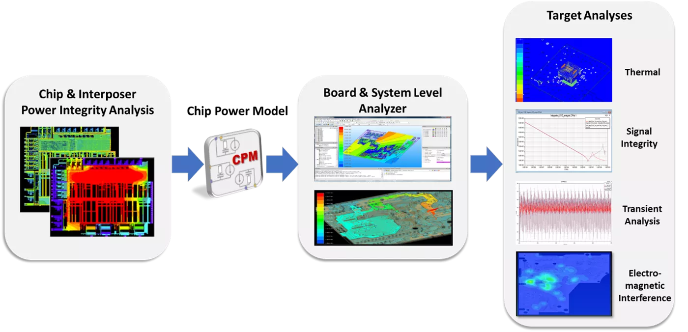
Customers require open and extensible platforms that support a broad range of analysis tools across many different abstraction levels – from device to chip to board to system.
The right simulation technology platform can significantly help. A shared platform that brings cross-functional engineering teams together for simultaneous, not sequential, multiphysics design can make it easy and seamless to collaborate across functional boundaries and support excellence in every aspect of power, performance, reliability and cost.
By balancing these foundational performance aspects with simultaneous optimizations of temperature, mechanical stress and other subtle effects, semiconductor engineering teams can position themselves as leaders, not followers, in the 3D-IC revolution.
Learn More at the Ansys IDEAS Digital Forum
Register for Ansys IDEAS Digital Forum on demand to learn more about 3D-IC best practices from leading industry experts (www.ansys.com/ideas).
John Lee is General Manager of the Electronics and Semiconductor Business Unit at Ansys.