
The latest MEMS and sensors advancements in markets ranging from displays to biotech and in key areas of manufacturing including sensor devices and fabrication came into sharp focus at the 2022 MEMS & Sensors Technical Congress (MSTC) in late April as more than 120 industry experts gathered in Berkeley, California to network and share cutting-edge innovations.
The MSTC agenda featured a diverse set of talks detailing many innovative new ideas. Two from the MEMS and Sensors for Better Living Session were particularly powerful:
 Lauren Otto, Ph.D., Director of Chip Realization at Mekonos, presented how she is leading an effort to re-engineer cells using nano-needles to deliver desired features to the nucleus of individual cells. Silicon nano-needles attached to a MEMS actuator can deliver a payload directly into a cell’s nucleus. MEMS actuators are uniquely suited to this application because they can be built on chip in arrays with controlled movement. The micro-meter size and scale can be tuned for the slight movement needed for the cell treatment. Early test results show a 5x improvement over current methods in getting cells to express the desired change.
 Bharath Takulapalli from iNanoBio has developed a vertical field effect cylindrical nanopore transistor (FENT) device that lowers the cost and greatly accelerates DNA sequencing to potentially move this testing to the point-of-care facility. Each substrate nanopore is surrounded by a cylindrical transistor gate structure. When DNA strands pass through these nanopores, the transistor gate bias is slightly modulated depending on which DNA base (A-C, T-G) passes through it. Each base causes a corresponding change in the source-drain current, which is measured. The strands pass through at 1 million strands per second, 1000x faster than today’s state of the art. The 5mm x 5mm FENT chip would have ~10,000 pores in one array – approximately 1000 times faster than the current protein-based nanopore option. The company is looking for partners to assist in advanced packaging, commercialization, microfluidics integration and packaging, low-power ASIC, and massively parallel computing.
In Session 2, MEMS for AR/VR Sensors, the following presenters focused on MEMS-based nontraditional display technologies for AR/VR and laser scanning.
 Wyatt Davis from Microsoft described the company’s Hololens 2 product that uses individual Red, Blue and Green (RBG) laser diodes combined with Micro Mirrors. Natural resonant frequencies can cause measurement artifacts in the Micro Mirror products, especially in higher resolutions with the use of a mirror for each resolution point. Most of this can be addressed by the design by, for example, using biaxial (both vertical and horizontal) MEMS mirrors. There are three options for the actuation: 1) Piezo electric; 2) Electrostatic; and 3) Electromagnetic. Piezo is emerging as the best choice for scanning mirrors for displays, particularly thin film piezo.
 Ulrich Hoffmann, CEO of OQmented, revealed his laser scanned-based depth sensing and displays for augmented reality, particularly popular with the excitement around metaverse applications. Each MEMS mirror is encapsulated in a glass dome, using an Aluminum Nitride (AlN) based actuator. The dome encapsulation enables 180° Field of View and 400 mirrors can be fabricated on a 200mm wafer. The Lissajous scanning method uses dual x-y MEMS mirror resonances to enable faster display and detection of an object compared to traditional raster scanning and is an excellent scanning method for facial recognition applications.
Two sessions featured talks on sensor processing and technology and illuminated several innovations in thinking and planning for efficient use of materials and methods, including the three below.
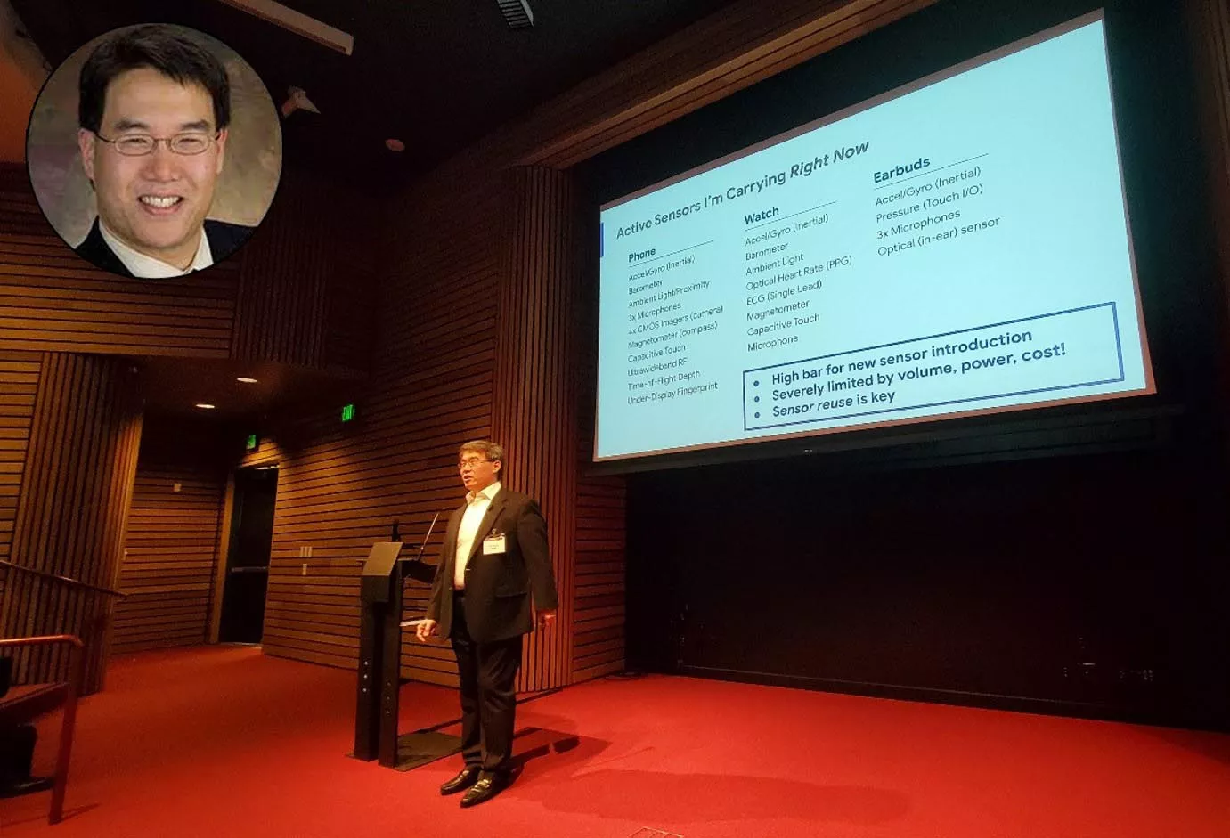
Sam Sheng of Google presenting at MSTC 2022
 Karel Cote, Senior MEMS Microfabrication Scientist at C2MI, proposed an advanced photolithography aligner that uses a Micro-optoelectromechanical system (MOEMS) that eliminates the need for physical photomasks. The MOEMS device uses a spatial light modulator (SLM) to create a virtual CAD based mask. This aligner can greatly reduce new MEMS product development cost by eliminating the costly photomasks, exposing only the needed areas on the wafer and running small wafer batches or even single wafers with more designs. Wafer-specific masks can also be handy for advanced packaging studies.
- Kimberly Harrison, AMFitzgerald, presented the results of its recent study of manufacturing glass-substrate based MEMS devices on large area flat panel display (FPD) glass substrates. The study revealed significant saving for the process compatible front-end steps due to efficiencies-of-scale. Compared to 200mm wafer, one Gen. 4.5 (730mm X 920mm) a-Si on glass panel could produce >20x the number of chips. The downside is that the back end of the processing would need to be done in a different facility. Robert Rodriquez, senior staff engineer at dpiX, followed with details on its foundry process capabilities at the company’s Colorado-based, Gen 4.5 FPD facility.
The following three presenters participated in Session 5, Sensors for Better Working.
 Thor Whalen, director of AI Research and Development at Analog Devices, presented how audio output from manufacturing equipment can be analyzed using artificial intelligence (AI) to identify early warning issues for preventative maintenance. The AI technology uses audio mosaics to greatly compress and remove unwanted sounds. Each sound can be characterized with alphabets that are then recognized, isolated and modified as needed.
 Lukas Baumgartel, application development engineer with INFICON, asked the attendees why conventional tool sensors only monitor tool health, but not really the process itself? He suggested that with some added sensors, fabricators can glean valuable knowledge of what is happening at the process level with real-time measurement capabilities. Using the example of deposition, with machine learning these sensors can enable precursor monitoring and provide a feedback loop to the process. Process owners can also modify the automatically learned confidence limits and set new boundaries as needed per actual wafer measurements, for example.
- Sam Sheng from Google answered his own question of “Have we reached peak sensors” in a comprehensive look at the sensors. Long story short, no. However:
- It will take creative thinking to replace the keyboard, tapping, clicking and typing input devices with something less intrusive.
- There is a very high bar for new sensor introductions with cost pressures and volume production restrictions. Reusing existing sensors (sensor fusion) is the shortest path to driving performance improvements, unless the new sensors are extremely novel.
 MSTC concluded with tours of several of the Berkeley laboratories and processing facilities. My fellow attendees were impressed with the scope, breadth and depth of the research and the facilities. It was great to be at a face-to-face event again and the event exceeded my expectations in every way.
To go into greater depth on any of these presentations, visit the event in the SEMI On-Demand platform. Registration is required.

SEMI MSIG thanks and recognizes the following sponsors, who made this event possible.
And the industry and media partners who helped promote the event.
MSTC is organized by MEMS & Sensors Industry Group (MSIG), a SEMI Technology Community. MSIG is dedicated to helping its members accelerate the adoption of MEMS and sensors worldwide. Membership is free with SEMI membership.
About the Author
 Petri Santala received his B.Sc. in Process Engineering at the Espoo University of Applied Sciences Finland. Santala has 25 years of experience in the semiconductor industry. He has worked for Okmetic since 1999 and held various positions related to R&D/process engineering, quality management, supplier management, and sales and applications. Santala currently works as a customer support manager for customers in North America.