Charles Shi, Principal, Senior Analyst, Needham & Company, LLC., recently offered an upbeat assessment of the electronic design automation (EDA), silicon intellectual property (IP) and services industries, or what SEMI refers to as the electronic system design (ESD) ecosystem. I attended his presentation during the 2022 Design Automation Conference, collocated this year with SEMICON West and found it fascinating.
His presentation, titled EDA Powers Through Semiconductor Cycles, is well worth taking the time to read.
Smith: You are optimistic that EDA will be okay through a downcycle, according to your recent presentation. Even so, are there steps companies can or should take to be prepared?
Shi: I do think EDA will continue to grow through a semiconductor downturn. R&D is the last place for semiconductor companies to cut costs as they do not want to miss the upturn, which will eventually come, by pausing new chip R&D during a downturn. However, the range of possibilities of the upcoming downturn is wider than the previous downturns.
 In the past, semiconductor downturns usually did not happen at the same time as macroeconomic downturns. A downturn in the West was often offset by continued growth of emerging markets such as China. This time, a chip downturn will likely coincide with a macroeconomic downturn because of inflation and the hangover of monetary and fiscal stimulus widely implemented by governments around the world to fight Covid.
What’s new this time is that the Chinese economy seems to be worsening in sync with the rest of the world. The EDA industry should stay optimistic, but should be closely monitoring the situation as a perfect storm of macroeconomic and industry dynamics may be brewing. Having said that, in 2008-2009, the last time when a very bad recession coincided with a chip downturn, EDA companies were still able to eke out some positive growth. Even in the worst scenario for this upcoming downturn, I believe EDA companies will do just fine. However, for both large and small companies, tightening the belt a bit is probably a prudent thing to do.
Smith: Do you see consolidation coming in EDA, much like you pointed out in the semiconductor space?
Shi: The EDA industry has largely consolidated to four large players and a number of small players. I think it has already consolidated as much as it can. After all, customers want competition and options. It is difficult for me to see further consolidation in the space. However, I do feel the industry needs to maintain a vibrant community of small EDA companies. The reason is that innovation, especially disruptive innovation, tends to come from smaller companies. It is beneficial to have a dynamic startup scene in EDA industry for both large and small EDA companies.
Large companies can continue to do what we call tuck-in acquisitions to scoop up interesting product ideas and talented engineers to keep innovations alive. Small companies can have M&A as a viable exit strategy besides going public, so the industry can continue to benefit from out-of-the-box thinking and brand-new ideas. While people may see EDA as a highly consolidated industry, the vitality and the health of the startup sphere is critical for the long-term growth of the industry in my view.
Smith: What about expansion into new markets and/or application spaces?
Shi: I am not trying to be specific here, as there are technical experts who can better articulate specific markets and applications. This may sound like very long-term thinking, but the fact that systems companies are coming in to do chip designs, and the industry is shifting from design to sell to design to use model tells me that system design and chip design is probably converging.
 The industry has talked about design-technology co-optimization, and hardware-software co-optimization. Current trends suggest that in the future, we could have even broader co-optimization all the way from electronics system on the top down to silicon process at the bottom. This is the so called digital twin concept in the new industrial era. This type of through-stack optimization will likely call on EDA companies to expand beyond just chip designs but entire electronics system designs.
Large companies are seeing this trend and are positioned for it. For example, Siemens acquired Mentor Graphics, which complements the Siemens industrial design and engineering software business. Ansys now does both engineering software and EDA, and an informal alliance between Synopsys and Ansys seems to be forming.
Furthermore, Cadence is acquiring engineering software companies in non-semiconductor spaces with a goal to build an integrated system design business under one roof. We will see how the industry landscape evolves, but the trend is becoming clear.
Smith: Do you consider the EDA and silicon IP ecosystem and partnerships to be strong enough to sustain a downturn?
Shi: I think the EDA companies are generally strong enough to sustain a downturn. Design IP companies may see some weakness because the economics of EDA and IP are slightly different.
Relative to EDA, we see varied profitability performance of IP companies, depending on the scale and scalability of their IP offerings. With the Federal Reserve Board tightening financial conditions, we see investors now have less appetite to put money in unprofitable businesses than the past 10 years when the Fed was easing financial conditions.

Once again, it is important for the IP community to work on the business model that has an increased return to scale and focus on IP products that can scale up. In other words, the IP business should be more like EDA business model, despite some intrinsic differences between them.
At the same time, I’m optimistic about the IP industry outlook and believe it will maintain double-digit growth going forward, because the value proposition is a beautiful one—IP provides the building blocks to chip designers, who do not want to reinvent the wheel but focus on a few things that will differentiate their designs. However, individual companies, especially smaller ones that are not profitable, may want to recalibrate their strategy and put more focus on product scalability and business profitability because the macro environment and financial conditions over the next few years will look very different from the past decade.
Smith: Coupling packaging and chip co-design has been a challenge for a number of reasons. What do you recommend doing to bring the two groups together?
Shi: This is not exactly a recommendation. Coordinating multiple parties, such as fabless companies, foundries, memory chipmakers, and Outsourced Semiconductor Assembly and Test (OSATs) seems to have been an issue in bringing the chip-package co-design together.
I believe foundries are seeing the problem and have been in the process of bringing the most advanced packaging and testing in-house for a decade. As another example, Intel recently talked about system foundry replacing the wafer foundry.
 At least from the manufacturing side of the ecosystem, it has proven to be a net plus for the industry to have wafer manufacturing and packaging under one roof, because then the established ecosystem of foundry, EDA and IP that have perfected the coordination mechanism for three decades can start to make a difference to push chip-package co-design ahead.
From time to time, you hear foundries express frustration about the adoption of 3D IC, but I’m optimistic that the existing foundry-EDA-IP ecosystem will solve the problem because of demand from fabless customers. This is similar to what has been happening in the manufacturing circle, where a tighter integration between chip and package manufacturing is happening. In the design circle, a tighter integration between chip and package design is the way to go.
Of course, the EDA industry needs to solve the problem of interoperability of tools, and the fabless industry may need to break the silos between different design teams. However, neither of these are new problems. Eventually, people will do the right thing and solve these problems.
Smith: Is the move by systems companies to make their own chips a long-term strategy or a short-term tactic?
Shi: This is a long-term strategy. At the root of it is the slowdown of Moore’s Law.
The slowdown of Moore’s Law first slows down the advancement of general-purpose chips, like CPUs. In the past, when Moore’s Law was iterating at a breakneck speed, a system company making its own chip was unlikely to be as fast as a chip company. Now, we are at a point when the incremental gains in power, performance and area from one node to the other are smaller than before and the cadence between two nodes is stretching out, such that general-purpose chips are no longer advancing as quickly as they once did.
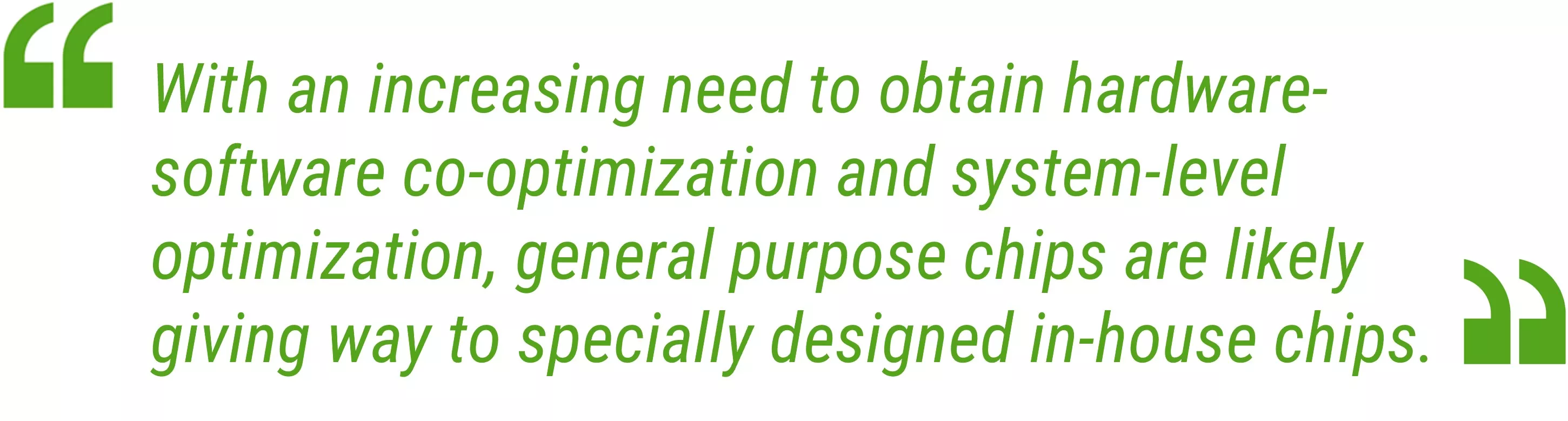
In addition, general-purpose chips typically aim to cover a lot of applications to maximize scale and minimize cost, but those chips do a suboptimal job for many applications. With an increasing need to obtain hardware-software co-optimization and system-level optimization, general purpose chips are likely giving way to specially designed in-house chips. The foundry, EDA and IP ecosystem are making it easier for systems companies to do designs. I do not see this is a fad.
Many years ago, people were talking about how the slowdown of Moore’s Law would make it easier for other chip manufacturers to catch up to TSMC. The opposite happened, and a lot of fabs have dropped out of the race. However, I would say this everyone can now catch up is probably a true statement for chip designers. It is interesting that in the early part of the semiconductor history, the ones that design chips are the ones that sell systems. We have come full circle.
Smith: Do you think the democratization of chip design is more than a tagline?
Shi: I don’t think it’s just a tagline. It sounds like an over-the-top motivational speech that everyone hates. But in chip design, general-purpose computing giving way to domain-specific computing is happening, because of the Moore’s Law slowdown. The one who knows the domain the best is the one who actually owns the systems.
 General-purpose chip companies don’t own the system. The systems companies do. They do not only have the motivation to in-source chip designs––they have the whole foundry, EDA and IP ecosystem to back them up.
Many of these systems companies have the financial resources to invest in chip designs. I think the chip design industry is not going to be more consolidated but more fragmented. Even for today’s leading semiconductor companies, you will hear more from them talking about custom designed products. They are also going in the direction of domain-specific computing. But eventually, I think those that own the systems will end up being the ones that own the chip designs. It may be a slow process to get there but current trends suggest it is just a matter of when not if.
Smith: Will the CHIPS Act have an impact on re-establishing a leading-edge domestic semiconductor manufacturing industry?
Shi: I think this question really ties to whether Intel can turn itself around. Literally speaking, TSMC is building leading-edge domestic semiconductor manufacturing in the U.S.
But I think from the government’s point of view, they do not just want the manufacturing capacity on U.S. soil but also the R&D capability on U.S. soil. To me, whether the U.S. can both have the capacity and the expertise domestically depends on whether Intel can turn itself around and regain the leadership. It is a big bet. I hope it works out but I am cautious whether the outcome will turn out to be what the policymakers expect. The world has provided enough bad lessons on government-driven industrial policies especially in semiconductors. I hope the U.S. can learn from Europe and China and spend the CHIPS Act money wisely.
Smith: What advice would you give to an EDA entrepreneur?
Shi: Focus on the products, and the scalability of your products. Think out of the box, move fast and break things. You may not realize how much the long-term health of the EDA industry depends on you.
About Charles Shi
Charles Shi joined Needham & Company in 2019. He became a research analyst in 2021 covering Semiconductors and Semicap Equipment. Prior to Needham, Shi spent six years at Applied Materials, where he started as a global product manager in the metal deposition products division, and later became a business development manager covering the division’s foundry accounts. Shi received a Ph.D. in materials science and engineering and an MBA from the University of California, Berkeley, and a bachelor’s degree from Tsinghua University.
Robert (Bob) Smith is executive director of the ESD Alliance, a SEMI Technology Community.