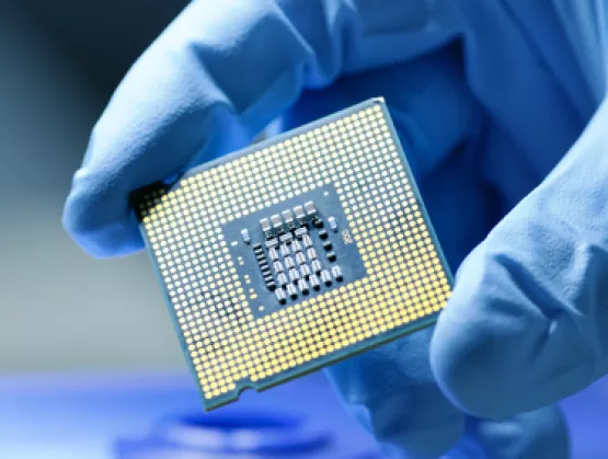
New system-on-chip (SoC) devices are driving new memory architectures and photonic interfaces, while specialized new intellectual property (IP) requires analysis down to the nanometer and atomic levels because of single nanometer process nodes. According to Babak Taheri, CTO and EVP of products at Silvaco, a leading EDA Software, semiconductor IP company, a member of SEMI and the ESD Alliance, a SEMI Strategic Association Partner, design technology co-optimization and proven IP are required for this analysis.
Taheri recently discussed atoms to systems in next-generation SoC designs with Nanette Collins ahead of ES Design West, co-located with SEMICON West, July 9-11 at the Moscone Center in San Francisco.
ESD Alliance: For years now, the assumption is that each new chip design is more complex than the last. Why are the latest SoC designs even more complex than before?
Taheri: New SoC devices for mobile phones, automobiles, intelligent edge nodes, big data compute and storage are adopting artificial intelligence and machine learning technologies. This is driving new compute, data flow, as well as memory architectures that are bandwidth-limited and some require photonic interfaces.
 One common denominator in present SoC design are the numerous blocks of IP. On average, over 85% of these blocks are reused. It’s cost-prohibitive to make these chips over and over again with new IP. According to some estimates, 90% of IP used in an SoC design by 2025 will be reused – only 10% is new technologies. That 10% is significant.
ESD Alliance: How so?
Taheri: Complex new technologies including flash memory, other advanced non-volatile memory technologies such as MRAM, RRAM and SoCs such as NVIDIA’s Xavier and Apple’s A12 use and reuse design IP at the architectural level.
New technologies mean new materials and new processes. Single nanometer process nodes require specialized new IP that needs to be simulated and analyzed down to the nanometer and atomic levels.
ESD Alliance: Does the atomic level changes the design equation?
Taheri: Yes, it does. Designers need to be able to simulate at the atomic level and understand properties of these materials, and how they behave in at-process and at-device levels. They need be able to simulate the material's nanometer geometries, how molecules behave and how they interact for device operations. When they put together a process and a device, they need to know how the pieces behave and simulate before production.
In other words, they run quite a few design experiments and quite a bit of simulation before they finalize the circuits and devices to silicon to save money.
ESD Alliance: It’s obvious design automation will continue to have a vital role in design.
Taheri: Yes, absolutely. Design technology co-optimization (DTCO) using TCAD solutions and proven design IP are needed to address the span from architecture to device and process physics.
The importance of simulation, emulation and design technology co-optimization, along with fully verified and proven IP for SoC design, cannot be overstated. As designers generate devices and processors, they take that up to circuit-level simulation and high-level simulation, schematic capture, extractions and back annotation. They can go from atoms to simulating systems to the ability to do that under the same umbrella in order to get better chips, better yield and lower cost.
Taheri’s talk Next Generation of SoC Design: From Atoms to Systems will be part of the Meet the Experts More than Moore session Tuesday, July 9, at 11:30 a.m. at the ES Design West SMART Design Pavilion. SEMICON West attendees are invited to Moscone Center’s South Hall to learn more about electronic system and semiconductor design and its links to the electronic product manufacturing and supply chain.
Register for ES Design West or SEMICON West.
 Babak Taheri is Silvaco’s CTO and EVP of products, has more than 25 years of design experience. His current role managing Silvaco’s Technology CAD (TCAD), electronic design automation (EDA) and IP product divisions makes him an expert on what’s needed for the design of next-generation system-on-chips (SoCs). Previously, he was the CEO and president of IBT working with investors, private equity firms, and startups on M&A, technology and business diligence. Babak received his Ph.D. in biomedical engineering from the University of California Davis with Bachelor of Science degrees in Electrical Engineering and Computer Science and Neurosciences. He has published more than 20 articles and holds 28 issued patents.
Nanette Collins is a public relations representative for the Electronic System Design Alliance.