“Thinner and Smaller” Continues to Dominate Packaging Industry
SAN JOSE, Calif. — December 14, 2015 — According to the newly released “Global Semiconductor Packaging Materials Outlook — 2015/2016 Edition,” the $18 billion semiconductor packaging materials market will undergo steady single-digit unit volume growth for many material segments through 2019, including laminate substrates, IC leadframes, underfill, and copper wire. Segments such as wafer-level packaging (WLP) dielectrics will experience stronger unit volume growth over the same timeframe. The new report by SEMI and TechSearch International covers laminate substrates, leadframes, bonding wire, mold compounds, underfill materials, liquid encapsulants, die attach materials, solder balls, wafer level package dielectrics, and thermal interface materials.
Packaging materials are a key enabler to increasing the functionality of thinner, smaller packages consumed in smart phones and other mobile products. Many options are currently available to meet form factor requirements for mobile products such as stacked-die chip scale package (CSP), land grid array (LGA) and fine pitch ball grid array (FBGA) packages, package-on-package (PoP), wafer-level package (WLP), Quad Flat No-lead (QFN) and other packages, using both wirebond and flip chip interconnects.
Key observations include:
- FO-WLP is emerging as a disruptive technology, changing the demand for the types of packaging materials used in the industry
- Need for WLP dielectric materials for multi-layer redistribution layers
- New materials for laminate substrates and underfill to pitch decreasing pitch and bump height trends in flip chip packaging
- Improved mold compounds for warpage control and package reliability
- For QFN packaging, cost optimization through enhanced designs and reduced plating area; higher lead counts (routable); improved power dissipation
- Continued growth in copper and silver wire
- Materials and processes compatible with tighter tolerances for higher density leadframes and substrate packaging, and for compact multi-die system-in-package (SiP) configurations
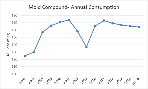
Constrained industry growth and the trend towards lower-cost electronics have reshaped the packaging material supplier landscape. Changes in material sets, the emergence of new package types, and cost reduction pressures have resulted in recent consolidation in various material segments. In addition, materials consumption in some segments is declining given the changes in package form factors and the trend towards smaller, thinner packaging (see Figure).

Source: SEMI and TechSearch International, Global Semiconductor Packaging Materials Outlook 2015/2016 Edition
The findings in the report are based on over 150 in-depth interviews conducted with semiconductor manufacturers, fabless semiconductor companies, packaging subcontractors, and packaging materials suppliers throughout the world. The report covers details about the industry growth and trends for the various material segments. Information includes market size, regional data, unit trends, and market share. It includes previously unpublished data on revenue, unit shipments and market shares for each packaging material segment; a five-year forecast of revenue and units from 2015 to 2019; supplier rankings (for key segments) and listing (including new players); and an analysis of regional market trends and size. All of the information was derived from the SEMI Global Packaging Materials Outlook from 2015 to 2019 produced by SEMI and TechSearch International. The report license is available for single user and multi users. SEMI members save 16 percent or more depending on types of license.
For more information about the report (Semiconductor Packaging Materials Outlook—2015-2016 Edition) and to order your copy, please click here.
About SEMI
SEMI is the global industry association serving the electronics manufacturing supply chains. Our more than 2,000 member companies are the engine of the future, enabling smarter, faster and more economical products that improve our lives. Since 1970, SEMI has been committed to helping members grow more profitably, create new markets and meet common industry challenges. SEMI maintains offices in Bangalore, Beijing, Berlin, Brussels, Grenoble, Hsinchu, Moscow, San Jose, Seoul, Shanghai, Singapore, Tokyo, and Washington, D.C. For more information, visit www.semi.org.
Association Contacts
Dan Tracy/SEMI
Phone: 1.408.943.7987![]() 1.408.943.7987 FREE
1.408.943.7987 FREE
Email: dtracy@semi.org
Deborah Geiger/SEMI
Phone: 1.408.943.7988![]() 1.408.943.7988 FREE
1.408.943.7988 FREE
Email: dgeiger@semi.org
# # #