MILPITAS, Calif. — April 18, 2018 — SEMI, the industry association representing the global electronics manufacturing supply chain, and TechSearch International today reported that the global semiconductor packaging materials market reached $16.7 billion in 2017. While slower growth of smartphones and personal computers – the industry’s traditional drivers – is reducing material consumption, the slowdown was offset by strong unit growth in the cryptocurrency market in 2017 and early 2018. Flip chip package shipments into the cryptocurrency market, while providing a windfall to many suppliers, are not expected to remain at high levels.
 The Global Semiconductor Packaging Materials Outlook shows that, despite growth in automotive electronics and high-performance computing, continuing price pressure and declining material consumption will constrain future material revenue growth to steady single-digits, with the materials market forecast to reach $17.8 billion in 2021. IC leadframes, underfill, and copper wire are among the materials segments that will see single-digit unit volume growth through 2021.
Laminate substrate suppliers participating in the sale of flip chip substrates for cryptocurrency saw volume increases in 2017, but this segment continues to be battered by increased use of multi-die solutions and the shift to wafer level packages (WLPs), including fan-out WLP, slowing growth. Wafer-level packaging (WLP) dielectrics and plating chemistry suppliers will experience stronger revenue growth as the adoption of advanced packaging continues.
Over the next several years, advances in the semiconductor materials market will present a number of opportunities driven by trends including:
- Continued adoption of FO-WLP including FO-on-substrate solutions with high density geometries down to 2µm lines and spaces
- Liquid crystal polymer (LCP) under consideration as a possible material option because of its good electrical performance and low moisture absorption, especially for mmWave applications such as 5G
- Adoption of low-cost package solutions such as MIS and other routable-QFN technologies
- PPF QFN volumes are rising with automotive applications, driving a requirement for roughened plating to deliver needed reliability
- Expansion of photoresist plating capability for selective plating of leadframes
- Thermally enhanced and high-voltage mold compounds for power and automotive devices
- Thermally conductive die attach materials other than solder die attach for power applications
Report highlights include:
- Laminate substrates represent the largest revenue segment of the materials market with more than $6 billion in sales for 2017.
- Overall leadframe shipments are forecast to grow at a 3.9 percent CAGR from 2017 through to 2021, with LFCSP (QFN type) experiencing the strongest unit growth, an 8 percent CAGR.
- Following five years of decline, gold wire shipments increased in both 2016 and 2017 though represent just 37 percent of the total bonding wire shipments in 2017.
- Liquid encapsulant revenues totaled $1.3 billion in 2017 with single-digit expected through 2021. LED packaging applications are driving the revenue growth over the forecast period though downward pricing pressures are a constant in the market.
- Die attach material revenues reached $741 million in 2017 with single digit growth to 2021. DAF materials will experience higher unit growth, though downward pricing trends continue.
- Solder ball revenues reached $231 million in 2017. The revenue outlook depends on fluctuations in metal pricing.
- The wafer-level plating chemical market was put at $263 million in 2017 with strong growth through 2021. RDL and Cu pillar will be the key growth segments.
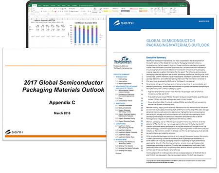
SEMI and TechSearch International, Inc. teamed up again to develop the 8th edition of the Global Semiconductor Packaging Materials Outlook, a comprehensive market research study on the semiconductor packaging materials market. Interviews were conducted with more than 130 semiconductor manufacturers, packaging subcontractors, fabless semiconductor companies, and packaging material suppliers to gather information for the report. The report covers the following semiconductor packaging materials segments: substrates, leadframes, bonding wire, mold compounds, underfill materials, liquid encapsulants, die attach materials, solder balls, wafer level package dielectrics, and wafer-level plating chemicals.
For more information and to purchase the report, click here.
About SEMI
SEMI® connects over 2,000 member companies and 1.3 million professionals worldwide to advance the technology and business of electronics manufacturing. SEMI members are responsible for the innovations in materials, design, equipment, software, devices, and services that enable smarter, faster, more powerful, and more affordable electronic products. FlexTech, the Fab Owners Alliance (FOA) and the MEMS & Sensors Industry Group (MSIG) are SEMI Strategic Association Partners, defined communities within SEMI focused on specific technologies. Since 1970, SEMI has built connections that have helped its members prosper, create new markets, and address common industry challenges together. SEMI maintains offices in Bangalore, Berlin, Brussels, Grenoble, Hsinchu, Seoul, Shanghai, Silicon Valley (Milpitas, Calif.), Singapore, Tokyo, and Washington, D.C. For more information, visit www.semi.org and follow SEMI on LinkedIn and Twitter.
Association Contact
Michael Hall/SEMI
Phone: 1.408.943.7988
Email: mhall@semi.org