3D NAND, 10nm, and DRAM are Driving Forces
SAN JOSE, Calif. ─ March 10, 2016 ─ Front-end fab equipment spending (including new, used, and in-house) is projected to increase 3.7 percent in 2016 (to US$ 37.2 billion) and another 13 percent in 2017 (to $42.1 billion) according to most recent edition of the SEMI World Fab Forecast. Fab equipment spending for 2015 ended almost flat ($35.9 billion), with a slight decrease of -0.4 percent year-over-year.
SEMI’s World Fab Forecast report presents details of fab-related spending through the industry and extends the outlook through the end of 2017. Fab equipment spending is expected to pick up slowly in the first half of 2016, and accelerate into the second half when momentum starts to build for 2017, with a return to double-digit growth rates (see figure 1).
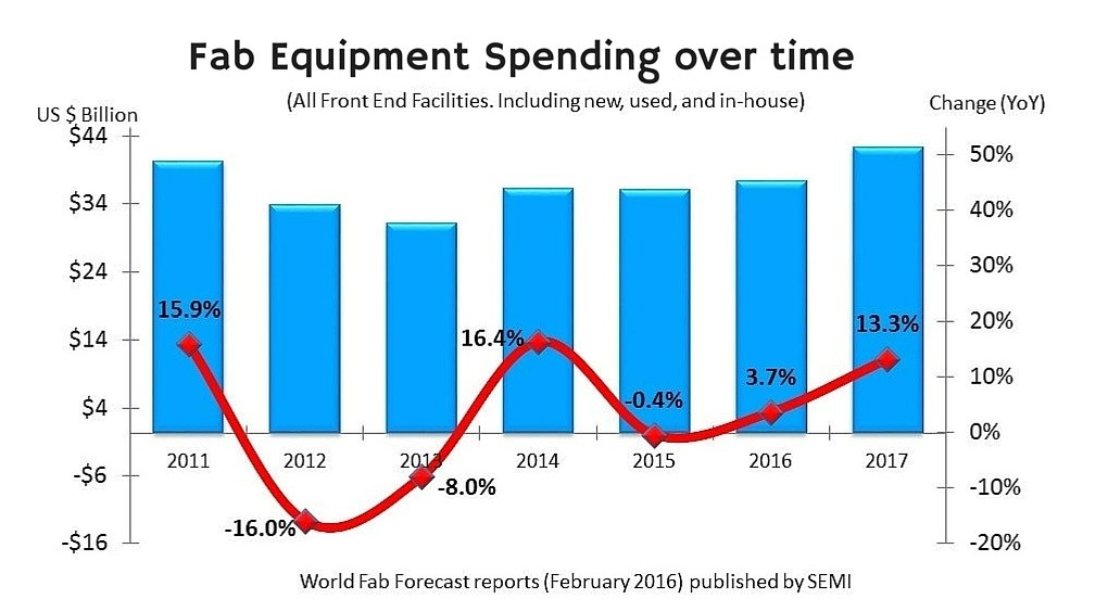
Figure 1: Fab equipment spending over time.
The biggest contributors to the growth are foundries, 3D NAND fabs, and companies beginning to equip and prepare for the 10nm ramp-up in 2017. Dedicated foundries continue to represent the largest spending segment. Spending for 2015 dropped slightly from $10.7 billion to $9.8 billion (-8 percent YoY), but is expected to increase by 5 percent in 2016 and almost 10 percent in 2017.
DRAM spending ranks second place after foundries. After a strong 2015, DRAM spending is expected to slow in 2016 (-23 percent) and increase again in 2017 by 10 percent.
In terms of spending growth rates, the big momentum comes from 3D NAND (including 3D XPoint). Spending doubled from about $1.8 billion in 2014 to $3.6 billion in 2015, 101 percent growth. In 2016, it will again rise to more than $5.6 billion (50 percent growth).
The increase in equipment spending is also supported by six companies, which are among the top 10 spenders globally. The six have announced plans to increase their respective capital expenditures in 2016, while the assumption for the largest spender, Samsung, is that capital expenditure will be less than in 2015.
Equipment spending growth for 2017 is also buoyed by new 24 facilities (excluding R&D) which began construction in 2015 or will begin construction this year. These projects are located around the world, including eight planned in China alone.
The industry has recently set records for mergers and acquisitions, and more are expected in 2016. The combined flat growth for semiconductor equipment spending in 2015 and slow growth in 2016 confirm a more mature industry. New technologies — new nodes and newer memory devices — will drive the increase in spending currently forecasted for 2017.
To learn how semiconductor manufacturing will look in 2016 and 2017 and additional details about capex for construction projects, fab equipping, technology levels, and products, order the SEMI World Fab Forecast Report. The report, in Excel format, tracks spending and capacities for over 1,100 facilities including over 60 future facilities, across industry segments from Analog, Power, Logic, MPU, Memory, and Foundry to MEMS and LEDs facilities. Using a bottoms-up approach methodology, it provides high-level summaries and graphs, and in-depth analyses of capital expenditures, capacities, technology and products by fab. Learn more about SEMI fab databases at: www.semi.org/MarketInfo/FabDatabase and www.youtube.com/user/SEMImktstats
About SEMI
SEMI® connects more than 1,900 member companies and more than a quarter-million professionals worldwide to advance the science and business of electronics manufacturing. SEMI members are responsible for the innovations in materials, design, equipment, software, and services that enable smarter, faster, more powerful, and more affordable electronic products. Since 1970, SEMI has built connections that have helped our members grow more profitably, create new markets, and address common industry challenges together. SEMI maintains offices in Bangalore, Beijing, Berlin, Brussels, Grenoble, Hsinchu, Moscow, San Jose, Seoul, Shanghai, Singapore, Tokyo, and Washington, D.C. For more information, visit www.semi.org and follow SEMI on LinkedIn and Twitter.
Association Contacts
Deborah Geiger/SEMI
Email: dgeiger@semi.org
Phone: 408.943.7988
Dan Tracy/SEMI
Phone: 1.408.943.7987
Email: dtracy@semi.org
# # #