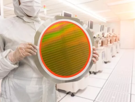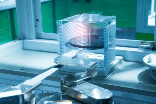
Semiconductors play an essential role in modern society by enabling ground-breaking technological advances. The manufacture of high-volume and advanced semiconductors requires the use of fluorinated chemicals known as PFAS. Representing the voice of SEMI members, I explained the important role of these substances and their “essential use” in the semiconductor manufacturing supply chain at a Chemical Watch conference for industry and European Union decision-makers on 3rd of December 2020.
In order to achieve the European Green Deal’s zero pollution ambition for a toxic-free environment, the European Commission announced in its recently published Chemicals Strategy for Sustainability its intention to restrict the use of the most harmful chemicals, except in cases where they are deemed essential for society. Per- and polyfluoroalkyl substances – known as PFAS – are the first group of chemicals facing regulatory scrutiny on this basis.
This begs the question: What chemicals should be characterized as essential for society and what uses will they encompass?
The key and enabling role of semiconductors in modern life
Semiconductors are essential and ubiquitous in our lives. They are integral to enabling modern society to function – driving advancements in mobile communication technologies for the smartphones and computers that help us work more efficiently and connect us with our loved ones. These benefits have never been more evident than in 2020 with billions of people finding themselves working and studying remotely and safely from home.
At the same time, technologies relying on semiconductors have been vital in the effort to combat COVID-19 – in ventilators, medical imaging devices and digital healthcare solutions. In addition, semiconductors will also enable the next leap in society to Industry 4.0 and as essential building blocks in connected and electric vehicles, artificial intelligence (AI) and quantum computing.
The Commissioner for Internal Market, Thierry Breton, has highlighted the strategic importance of semiconductors in achieving European digital sovereignty (for instance, in his speech at Hannover Messe Digital Days), and the EU’s New Industrial Strategy[1] also points to the importance of semiconductors and microelectronic systems.
What must also be appreciated are the cost and complexity of producing these valuable technologies. Setting up a cutting-edge fabrication plant with the hundreds of pieces of semiconductor manufacturing equipment typically required can cost around €15 billion.[2] A single semiconductor manufacturing tool typically consists of millions of articles, and a typical fab may house several hundred pieces of equipment. Furthermore, according to SEMI estimates, the fabrication of semiconductor wafers requires approximately 500 highly specialized process chemicals. In many cases, these processes, equipment and facilities rely on the unique properties offered by PFAS.
 “SEMI has worked diligently to highlight the strategic importance of semiconductors in achieving European digital sovereignty, and we are pleased that the critical role of microelectronics has been fully recognized by the EU and Member States. Fluorinated chemicals are essential for semiconductor manufacturing.
"These specific chemicals are necessary due to their unique properties, and no alternatives are currently available that can adequately provide the functional properties required in semiconductor manufacturing. The essential use concept, therefore, must enable technological innovation, must apply across the entire supply chain, and must enable EU’s critical infrastructure and strategic objectives.”
What are PFAS, and why and where are they used in semiconductor manufacturing?
PFAS are a broad and highly diverse group of substances with unique properties and characteristics. The Organisation for Economic Co-operation and Development (OECD) has compiled a list of approximately 4,700 substances,[3] a handful of which are used in the semiconductor manufacturing industry. These very specific chemicals are necessary due to their unique and unparalleled properties that enable them to be used in the demanding conditions of semiconductor manufacturing.
Semiconductor chemicals
At the very core of semiconductor manufacturing is the photolithography process, where microscopic geometric patterns are transferred onto a film or substrate. Photolithography specialty formulations containing fluorinated compounds are used in various steps of this process to ensure quality and reduce the probability of defects. PFAS must be used due to their low surface tension and compatibility with other chemicals. PFAS are typically no longer present in the finished product. However, there are applications where PFAS are present in the final semiconductor device, particularly in imaging semiconductors used in cameras, displays and some medical devices, amongst others.
Semiconductor manufacturing equipment
 PFAS are also essential to semiconductor manufacturing equipment and factory infrastructure. The exceptional combination of their heat and chemical resistance and their chemical inertness allows fluoropolymers to be used both in equipment components (tubing, gaskets, containers, filters, etc.) and lubrication (such as various oils and greases). These same properties are also needed to ensure the functioning of the surrounding infrastructure. Finally, some fluorinated gases, which are already regulated by specific legislation,[4] are used as refrigerants and to clean the facilities.
These are a handful of examples of how PFAS are used in semiconductor manufacturing. Today, there is no other way to undertake these processes or to build semiconductor manufacturing equipment without PFAS. No alternatives are currently available that can adequately provide the functional properties required. Even if alternative chemicals and technologies were discovered today, due to the extremely complex qualification process throughout the value chain, it would take another 15 years to deploy them in high-volume manufacturing. Therefore, continued access to PFAS is a prerequisite for high-volume and advanced semiconductors. Lack of continued access to PFAS could lead to an inability to produce and supply the EU with semiconductor manufacturing technology.
How should we think about essential uses?
Regulators have started to think about what uses of PFAS are essential and in which cases their use should be allowed. In developing this concept, there are a few aspects to keep in mind.
Essential use must enable, not hinder, technological innovation
First and foremost, the essential uses concept should enable continued technological innovation instead of acting as a hindrance. Semiconductors and manufacturing technology are constantly evolving and becoming more diverse to help meet increasing societal demands. What we see as innovative today may be commonplace in the future, while future innovations may be unimaginable today. We must therefore be careful not to accidentally limit our future potential for innovation.
Essential use must apply across the entire supply chain
Secondly, classifying a use as essential should apply throughout the entire supply chain. We must, for example, avoid defining semiconductors as essential while classifying the semiconductor manufacturing equipment and chemicals used to produce semiconductors as not essential. In the semiconductor manufacturing supply chain, where one manufacturer can have up to 16,000 suppliers, this risk is evident.[5]
Essential use must enable critical infrastructures and the EU’s strategic objectives
Finally, we should keep Europe’s societal priorities in mind. The EU needs to be able to maintain and protect its critical infrastructures. Similarly, we should not lose sight of the EU’s strategic objectives of a green and digital Europe.
Semiconductors, in conjunction with their corresponding manufacturing equipment and chemicals, are essential technologies in everyday life and the backbone of the EU’s strategic value chains. Manufacturing semiconductors is a very expensive and complex process that would not be possible without the unique properties of PFAS, making them essential to achieving the EU’s strategic objectives today – whether the European Green Deal or digital autonomy – and in the future. Therefore, we must ensure that essential uses will enable the continued use of PFAS in semiconductor manufacturing.
The SEMI presentation delivered at the Chemical Watch event can be accessed here.
Emir Demircan is director of Public Policy and Advocacy at SEMI Europe.
[1] “The EU will also support the development of key enabling technologies that are strategically important for Europe’s industrial future. These include robotics, microelectronics, high-performance computing and data cloud infrastructure, blockchain, quantum technologies, photonics [etc.]”
[2] Emerging technologies in electronic components and systems (ECS) Opportunities Ahead – A study by DECISION, 2018 for the European Commission
[4] Regulation (EU) No 517/2014, “F-Gas Regulation”
[5] SIA & Nathan Associates, 2016, https://www.semiconductors.org/wp-content/uploads/2018/06/SIA-Beyond-Borders-Report-FINAL-June-7.pdf