Negotiating the industry’s deglobalization, opportunities for a more resilient Europe
This article is the first of a two-part series on the Industry Strategy Symposium (ISS) Europe.
Over 200 delegates gathered in Vienna for the Industry Strategy Symposium (ISS) Europe at a time of contrasting expectations for the region’s semiconductor industry. On one hand, the industry is filled with optimism and excitement about the promise of the European Chips Act to fuel growth the rest of this decade. On the other, challenges abound over the shorter term, ranging from continued supply chain disruptions due to the Russia-Ukraine conflict and other geopolitical tensions to forecasts of a sharp slowdown in the global semiconductor industry stretching throughout the end of this year.
But speakers at the symposium were focused squarely on the influence of the EU Chips Act on the strategic direction of Europe’s semiconductor industry through 2030 and the legislation’s potential as a powerful instrument to strengthen the industry. Over two days of expert presentations and panel discussions, the symposium saw a balance of opinions from industry leaders, government, and European Commission officials on the top priorities for action.
Strategy track: exploring opportunities for the European semiconductor value chain
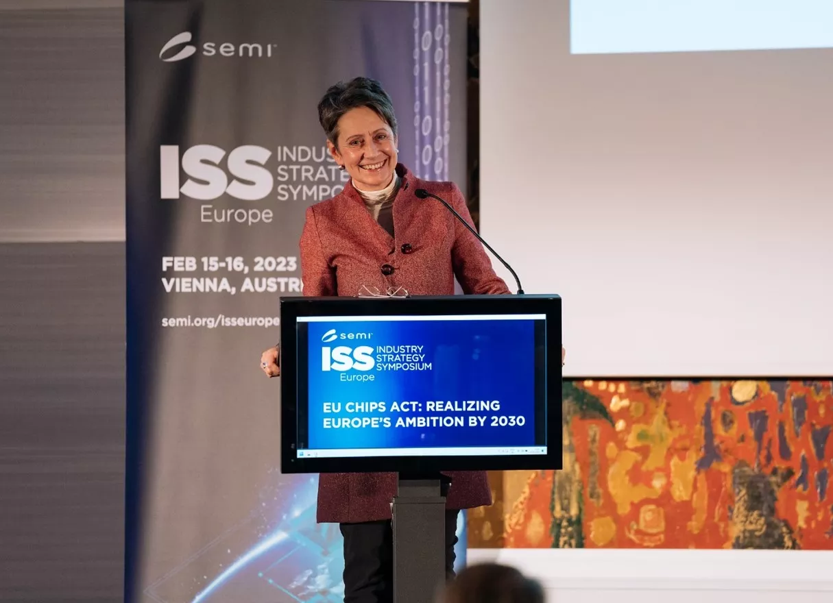
What emerged from the presentations was a shared belief in the scale of the opportunity for Europe’s semiconductor industry as reflected in opening remarks by SEMI Europe President, Laith Altimime. He described the current moment as “the most exciting time that Europe’s semiconductor industry has ever experienced,” citing Intel’s plans to build three fabs in the European Union, the €5 billion investment by Infineon Technologies in a new fab in Dresden, Germany, commitments by Wolfspeed, and STMicroelectronics with GlobalFoundries, and the Spanish government’s decision to invest €12 billion in the domestic semiconductor industry.
“This amounts to a great endorsement of Europe’s leadership in semiconductors,” Altimime said before highlighting the areas of collaboration key for Europe’s share of the global semiconductor market to reach 20% by 2030, up from just 8% today – a goal set by the European Commission.
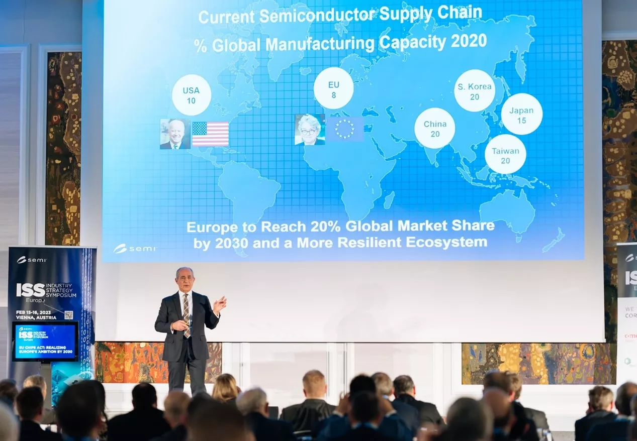
Laith Altimime, President of SEMI Europe
The EU Chips Act has increased the scale of the growth potential for Europe. Francisco Ibanez, Deputy Head of Unit for the Electronics Industry at the EC, explained the genesis of the act: While Europe’s electronics industry leads in some sectors, such as automotive and industrial equipment, it is completely absent in others, such as computing and the mobile phone.
“Unfortunately, the sectors in which we have no presence make up more than 50% of the entire market, and the scope for Europe to increase its share in those it already dominates is limited,” Ibanez said.
Francisco Ibanez, Deputy Head of Unit for the Electronics Industry at the European Commission
He said the EU strategy is to foster disruptive markets, especially advanced technologies and industry segments such as artificial intelligence (AI), 6G mobile, and Internet of Things (IoT) – in which a pioneering Europe can take an early and strong position. This is the context for the introduction of the EU Chips Act and its planned €80 billion investment in Europe’s semiconductor industry across design, innovation, manufacturing and packaging to “be sure that the EU is really committed to this industry,” Ibanez said. The act’s key provisions include investments in the following.
- Pilot lines to provide start-ups and semiconductor entrepreneurs with access to advanced technologies such as CMOS process technology down to 2nm, FD-SOI down to 10nm, and Advanced Heterogeneous System Integration (AHSI) packaging technology
- An online portal to give developers access to state-of-the-art chip design tools
- A Chips Fund to facilitate access by start-ups and SME’ to seed and development capital
Michael Wiesmüller, Head of Department of Key Enabling Technologies for Industrial Innovation in the Federal Government of Austria, provided a local perspective on the way government and the industry can work together to stimulate growth.
“We already have a highly developed semiconductor sector, thanks to the presence of Infineon, ams OSRAM, NXP, Bosch, STMicroelectronics, and others,” he said. “The number of employees in the sector has risen by 50% since 2016 to 72,000, and Austria ranks fourth in the EU for the number of patents it creates – a very strong performance in light of our small population.”
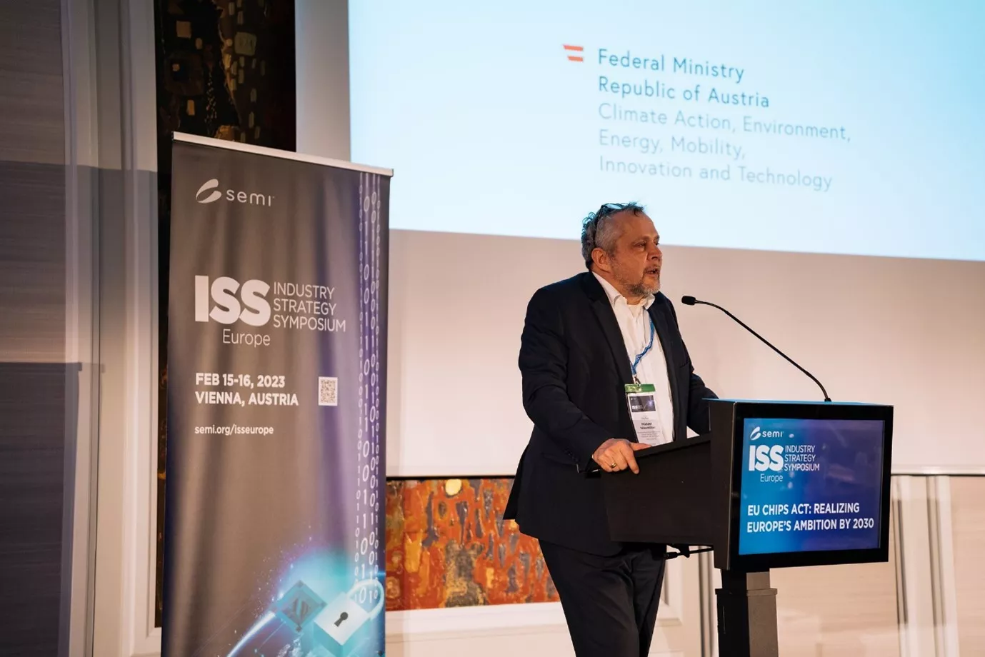
Michael Wiesmüller, Head of Department of Key Enabling Technologies for Industrial Innovation in the Federal Government of Austria
Today, the Austria government is leading efforts to expand its semiconductor sector, including its establishment of Silicon Austria, a technology organization with a focus on increasing R&D resources. While Austria is a small country with an outsized semiconductor sector, Wiesmüller said the region can offer “a growing sense of assurance about the leadership of Europe in segments of the semiconductor industry, and about the potential for it to grow.”
Market analyst Malcolm Penn, founder and CEO of Future Horizons, tempered the upbeat messages with a note of caution about the short-term outlook. He noted that the industry’s economic dynamics are very predictable and characterized by “boom-bust cyclicality.” Penn said the industry is now in recession: Future Horizons’ forecast is for a decline in global semiconductor industry revenue of 22% in 2023 to $447 billion. Penn noted, “There are no signs of growth currently – although in historic terms, this is actually quite a benign downward turn of the cycle.” Penn’s counterpart at consultants YOLE Intelligence, Guillaume Girardin, was equally sure that “2023 will be a tough year for the semiconductor market.”
In the long term, however, Penn remains optimistic about the industry. He gave clear advice to semiconductor industry executives: ”Double down on R&D, invest your way out of recession, and develop the products of the future now. The industry’s 17th upturn is just around the corner.”
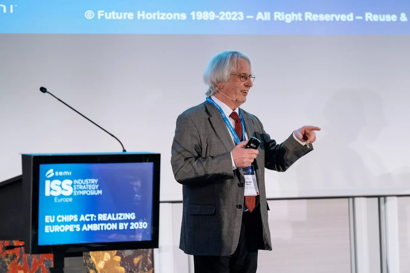
Malcolm Penn, Founder and CEO of Future Horizons
Vision for Europe 2030: negotiating the industry’s deglobalization
Some forecasts call for the global semiconductor industry to double in size to $1 trillion in revenue by 2030. But Michael Alexander, partner at the Roland Berger Advanced Technology Center, said the benefits of the boom will not be shared across the global industry. “Deglobalization has already started,” he said, noting that the trend is fueled by geopolitical conflict, particularly the Chinese military threat to Taiwan’s independence, and the effect of U.S. sanctions on the supply of advanced semiconductors and fabrication equipment to China. He referred to Apple’s shift out of China, the reduced number of the company’s Chinese manufacturing sites by 31% and increasing its U.S. manufacturing locations by 29%. ”Companies are already reshoring and changing their supply chains,” Alexander said.
In a panel discussion about the Vision for Europe 2030, Christin Eisenschmidt, Managing Director, VP and General Manager of Intel Europe, cited deglobalization as a reason for Intel’s expansion of manufacturing capacity in Europe. “In global semiconductor manufacturing, the U.S. and Europe only do 20%, while 80% is in Asia. This is not a good situation, so we want to help Europe to rebalance. And this aim is realistic because the ecosystem in Europe has a lot of momentum and a lot of potential.”
Analog Devices, another U.S.-headquartered semiconductor manufacturer with a large footprint in Europe, has operations in Ireland for almost 50 years, said Leo McHugh, the company’s VP for Industrial Automation and Technology. “The next wave of investment in Ireland recognizes that no company can do everything on its own. So, we have created a ‘Catalyst’, a new organization to bring us together with our customers and their customers. This enables us to develop more complete solutions and tame the complexity of today’s technology.”
Echoing the need for Europe-wide collaboration in response to deglobalization, Jo De Boeck, EVP and Chief Strategy Officer at research technology organization imec, said the focus of the EU Chips Act should be wider than just wafer fabrication. He called for “full-stack innovation, from materials up to applications. This means embracing all the technologies of the future, including wide bandgap semiconductors, quantum computing and photonics, neuromorphic computing, and implementation with a range of materials and chip architectures. And to achieve this, we need to be pan-European. We know how to work together – the personal networks in Europe are very strong. But we have to be international to achieve successful innovation.”
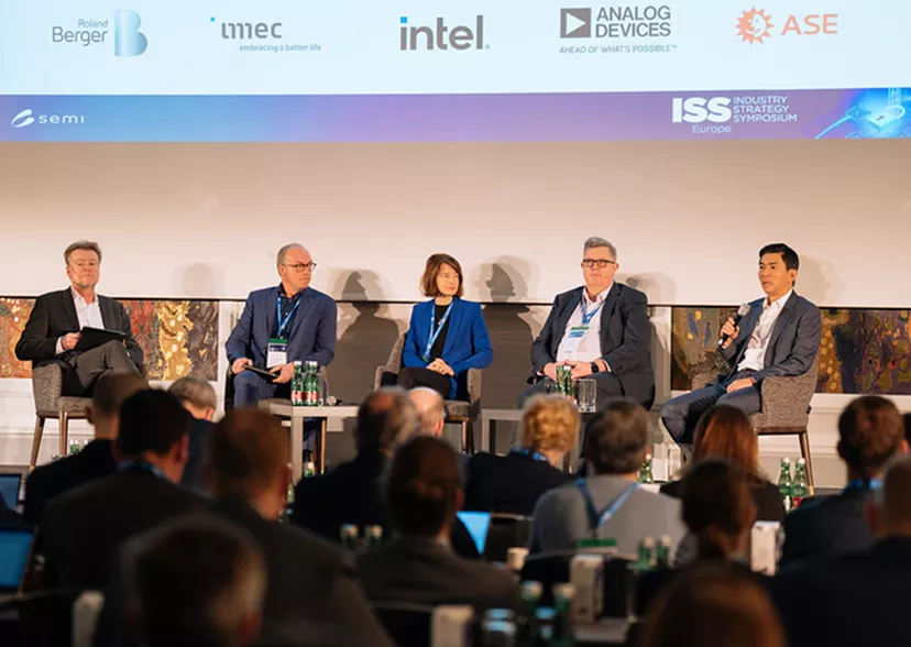
Left to right: Moderator, Michael Alexander, Partner at the Roland Berger Advanced Technology Center; Panelists: Jo De Boeck, EVP and Chief Strategy Officer at imec; Christin Eisenschmid, Managing Director and VP Europe Ecosystem Strategy at Intel Germany; Leo McHugh, VP Industrial Automation Technology at Analog Devices; Yin Chang, SVP, Sales and Marketing at ASE, Inc.
According to Yin Chang, SVP of Sales and Marketing at ASE, Inc., the largest Outsourced Semiconductor Assembly and Test (OSAT) company, De Boeck’s emphasis on the “full stack”, including packaging, is critically important. ”ASE has a footprint in Poland, and our vision is to keep in Europe for packaging as many of the wafers that are fabricated in Europe as possible, so that the finished chips can be used by European OEMs.”
The panel discussion ended with a call from Michael Alexander for Europe to build its semiconductor sector with much greater urgency, and to invest significantly larger sums than currently planned. He told delegates, “The US and China are paranoid about semiconductors. Europe needs to be paranoid about semiconductors as well.”
Seizing the opportunities: disruptive technology roadmap
As Laith Altimime noted during his opening address, for the Europe’s semiconductor industry to grow, it must draw on the region’s strengths across the entire value chain. His admonition was reflected by speakers in their views about the potential for disruptive technologies such as novel semiconductor equipment, emerging materials, and next-generation semiconductor architectures to support future models of computing.
Home to a fabrication equipment giant ASML, Europe is also a seedbed for innovation in semiconductor fabrication. Mathias Tomandl, Head of Customer Accounts and Projects Operations Division at IMS Nanofabrication, offered an example: his company’s electron multi-beam mask writer technology, which has powered its leadership of the market for mask writers for leading-edge processes. IMS equipment reduces the writing time for a complex mask from 70 hours to less than 12 hours while enabling the production of more precise patterns.
Mathias Tomandl, Head of Customer Accounts and Projects Operations Division, IMS Nanofabrication
Accelerating time-to-market was also the subject of a presentation from Dionys van de Ven, President of Comet Yxlon, whose innovative X-ray inspection technology dramatically reduces scan time in the optical inspection of semiconductor devices in production. “We enable innovations to get to market faster because you can find killer defects in a chip very early in production ramp-up, when they can be more easily and cheaply remedied,” van de Ven said. He added that Comet Yxlon’s x-ray inspection solutions not only reduce scan time, but also provide actionable information in minutes by using automated defect recognition solutions.
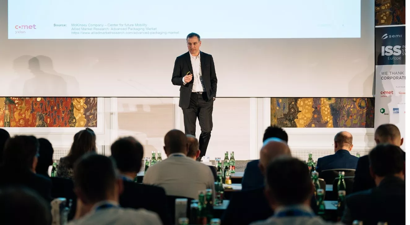
Dionys van de Ven, President of Comet Yxlon
European companies are also leading the development of disruptive technology in the field of semiconductor materials. Guillaume Girardin of YOLE highlighted compound semiconductors as a valuable focus for research and development – he forecast a 16% CAGR for the technology from 2021 to 2027.
Pierre Barnabé, CEO of SOITEC, said his company is taking advantage of this growth opportunity with its SmartSiC™ technology. The silicon carbide (SiC) wide bandgap semiconductor material is already increasing the efficiency and reducing the size of power systems in electric vehicles and their chargers. Barnabé explained that SOITEC’s development of the SmartSiC substrate offers far higher efficiency than SiC on its own. “Top tier automotive OEMs see SmartSiC substrates as a game changer for the electric vehicle market,” he noted.
Sabine Herlitschka, CEO of Infineon Austria, and Michael Anfang, EVP of sales and marketing at STMicroelectronics, confirmed that the leading semiconductor manufacturers in Europe are now making substantial investments in the design and fabrication of ultra-efficient SiC and gallium nitride (GaN) semiconductor products and technologies. “We are scaling up capacity to meet the real demand for the power semiconductors that will provide the energy improvements the world needs,” Herlitschka said.
Sabine Herlitschka, CEO of Infineon Austria
Steven Latré, Fellow at imec, told delegates that the development of new AI and machine learning applications called for the full-stack approach that his colleague Jo De Boeck had described. Latré said imec is exploring new computing architectures better adapted to AI workloads than today’s systems and raised the possibility of developing “neuro-inspired systems, because the human brain is much more efficient than today’s AI models." Embodying this type of innovative thinking at imec are its experimental µBrain and µBrain-X chips, which have reduced power consumption 100x in gesture detection compared to today’s state-of-the-art neural networking chips.
Architectural innovation is also bearing fruit in form of the Qu-Pilot project and was thetopic of a talk by Mika Prunnila of Finland’s VTT Technical Research Center. Backed by EU funding and involving cross-Europe collaboration among research organizations, academics, and companies including Infineon, the Qu-Pilot project is intended to bridge the gap between the R&D community and commercial-scale quantum chip manufacturing.
Prunnila noted that U.S. companies such as Google, IBM, and Intel are investing heavily in the hardware required for quantum computing. Qu-Pilot will give European start-ups and SMEs access to the expensive equipment and tools needed to fabricate quantum processors. “This is a critical stage in the race to lead in the global computing and chip markets,” he said.
A memorable year for ISS Europe
Leonard Hobbs, Chair of the ISS Europe committee and General Manager of MIDAS Ireland, said during his closing, "I am honored to chair this year's event and was really impressed by not only the high number of attendees who had made the journey to Vienna, but also by the level of enthusiasm and energy amongst the presenters and delegates. The ambition of Europe, as articulated in the EU Chips Act, and the associated optimism for Europe's bright future in semiconductors was evident in the positive atmosphere of this year's conference."
Leonard Hobbs, Chair of the ISS Europe committee and General Manager of MIDAS Ireland
Cassandra Melvin is senior director of Business Development and Operations at SEMI Europe.