downloadGroupGroupnoun_press release_995423_000000 copyGroupnoun_Feed_96767_000000Group 19noun_pictures_1817522_000000Member company iconResource item iconStore item iconGroup 19Group 19noun_Photo_2085192_000000 Copynoun_presentation_2096081_000000Group 19Group Copy 7noun_webinar_692730_000000Path
Skip to main content

Atomic Layer Deposition Expected to Grow to Meet Demand for More-than-Moore Devices and Applications

Atomic Layer Deposition (ALD) players are poised to seize a new growth opportunity after the chip shortage pushed manufacturers to announce fab capacity expansions worldwide. Driven by the wafer production volume increase, ALD solutions are now expected to grow and enter the MtM devices market.

Industrial Atomic Layer Deposition for Image Sensors and Light Sources

SEMI spoke with Dr. Mikko Söderlund, sales director for Beneq’s semiconductor business, about trends in Atomic Layer Deposition (ALD) applications. Söderlund shared his views ahead of his presentation at SEMI MEMS & Imaging Sensors Summit, 25-27 September, 2019, at the WTC in Grenoble, France.

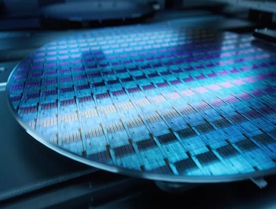
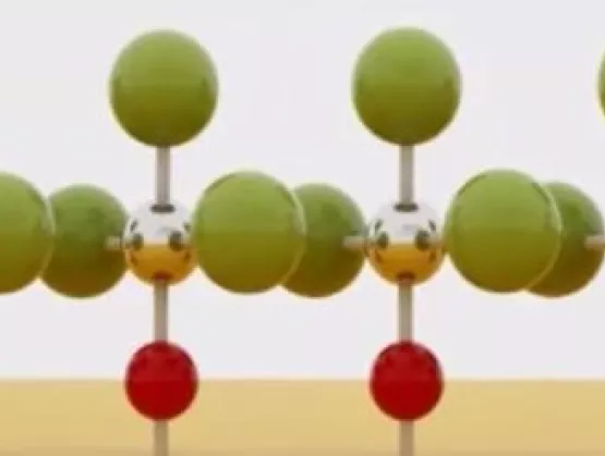
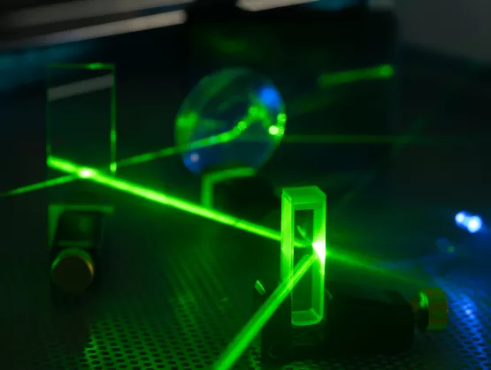
Zero Energy Connection (0eC) - A New Way to Transfer Data

SEMI met with Erez Halahmi, VP at 0eC SA, to discuss a new way to transfer information not only between chips but also between servers to reduce power consumption while boosting performance. The two spoke ahead of his presentation at the 3D & Systems Summit, 28-30 January, 2019, in Dresden, Germany.

Future Shines Bright for European Photonics Industry

SEMI met with Dr. Jose Pozo, director of Technology and Innovation at EPIC (European Photonics Industry Consortium), to discuss how 3D packaging applications and heterogeneous integration trends are shaping the European technology landscape.