
SEMI Standards form the foundation for innovation in the microelectronics industry. The SEMI Standards process has been used to create more than 1,000 industry approved standards and guidelines, based on the work of more than 5,000 volunteers.
SEMI Standards directly connect to better business results by seamlessly connecting the thousands of companies supplying millions of different parts to the electronics manufacturing ecosystem. Standards enable systems to work together, think together, and innovate together.
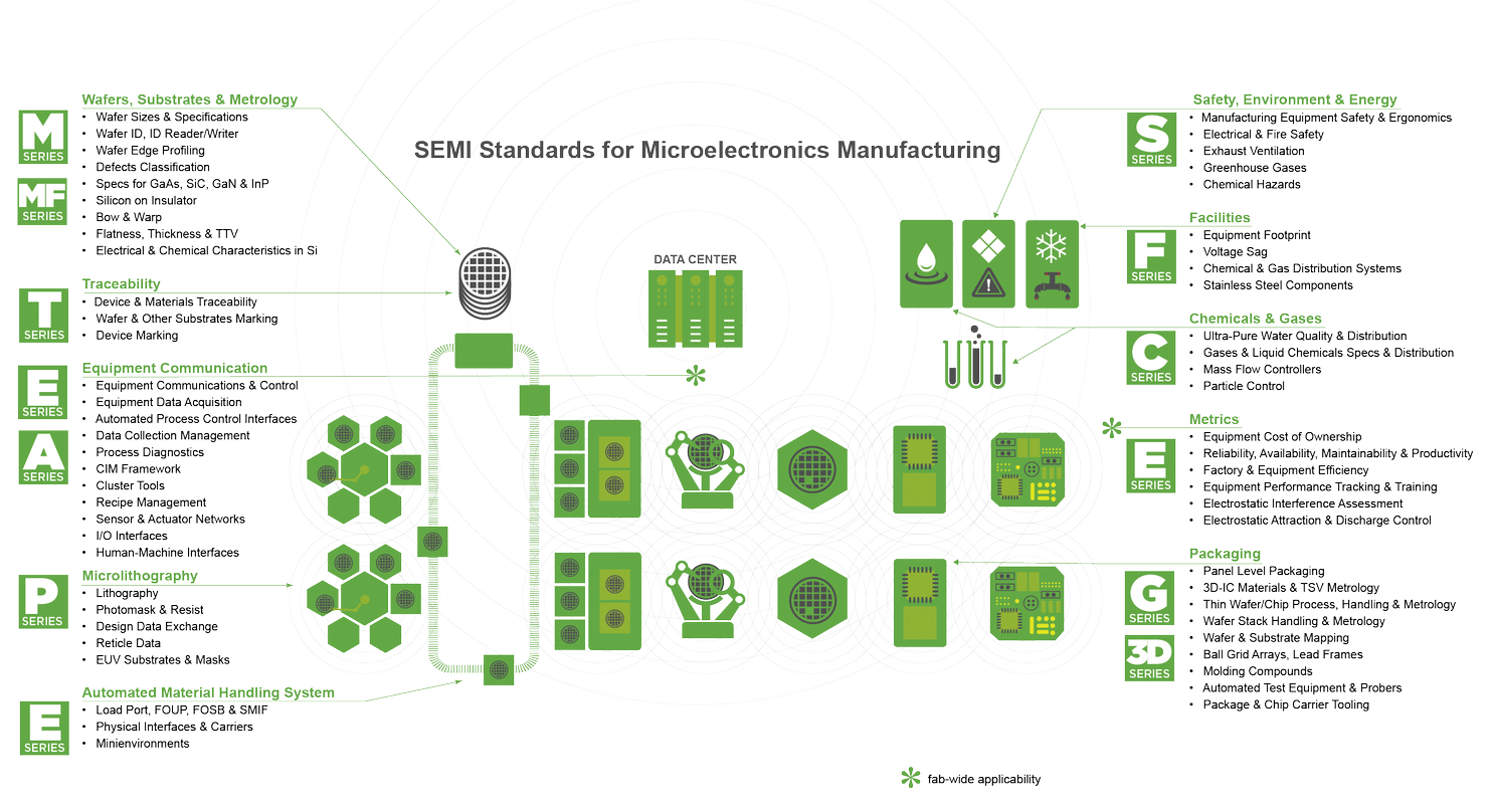

Packaging Related Semi Standards Committees
- 3D Packaging & Integration
- Automation Technology
- Information & Control
- Physical Interfaces & Carriers
- Traceability
If you are interested in participating in any of the Standards Committees, register below.
Critical SEMI Standards For Packaging
3D Stacked IC
- SEMI 3D1 - Terminology for Through Silicon via Geometrical Metrology
- SEMI 3D3 - Guide for Multiwafer Transport and Storage Containers for 300 mm, Thin Silicon Wafers on Tape Frames
- SEMI 3D6 - Guide for CMP and Micro-Bump Processes for Frontside Through Silicon Via (TSV) Integration
- SEMI 3D8 - Guide for Describing Silicon Wafers for Use as 300 mm Carrier Wafers in a 3DS-IC Temporary Bond-Debond (TBDB) Process
- SEMI 3D11 - Terminology for Through Glass Via and Blind Via in Glass Geometrical Metrology
- SEMI 3D12 - Guide for Measuring Flatness and Shape of Low Stiffness Wafers
- SEMI 3D22 - Guide on Measurements of Openings and Vias in Glass
Automation Technology
- SEMI A1 - Specification for Production Equipment Smart Connection Interface (PESCI)
- SEMI A2 - Specification for Surface Mount Assembler Smart Hookup (SMASH)
- SEMI A3 - Specification for Printed Circuit Board Equipment Communication Interfaces (PCBECI)
Factory Automation (Hardware)
- SEMI E181 - Specification for Panel FOUP for Panel Level Packaging
- SEMI E182 - Specification for Panel FOUP Loadport for Panel Level Packaging
Packaging
- SEMI G1 - Specification for Cerdip Package Constructions
- SEMI G3 - Specification for Sidebrazed Laminates
- SEMI G4 - Specification for Integrated Circuit Leadframe Materials Used in the Production of Stamped Leadframes
- SEMI G8 - Test Method for Gold Plating
- SEMI G9 - Specification for Stamped Leadframes for Plastic Molded Dual-in-Line Semiconductor Packages
- SEMI G10 - Standard Method for Mechanical Measurement of Plastic Package Leadframes
- SEMI G14 - Guideline for Specifying the Dimensions and Tolerances Used to Manufacture Plastic Molded Dip Package Tooling
- SEMI G99 - Specification for Flowability of Encapsulation Materials for Wafer Level Packaging and Panel Level Packaging