June 17, 2026 - June 19, 2026
#3DSummit
Time
8:30 am - 7:00 pm PDT
Location
Hilton Dresden Hotel
An der Frauenkirche 5
01067 Dresden
Germany
Thank You for a Successful 3D & Systems Summit 2026!
On behalf of SEMI, the SEMI Europe team extends our sincere appreciation to all sponsors, committee members, speakers, attendees, media partners, and social media followers of the 3D & Systems Summit 2026.
A special thank you to our SEMI Europe members for their participation and ongoing collaboration throughout the year. Your engagement and support drive meaningful discussions and innovation in the semiconductor industry.
We look forward to welcoming you again next year!
3D & Systems Summit 2027
📅 June 23-24, 2027
📍 Grenoble, France
Stay tuned for more details!
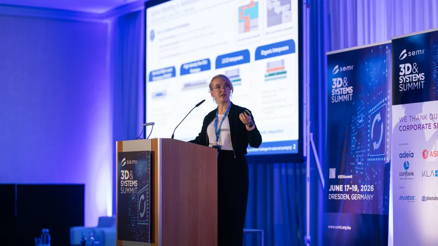
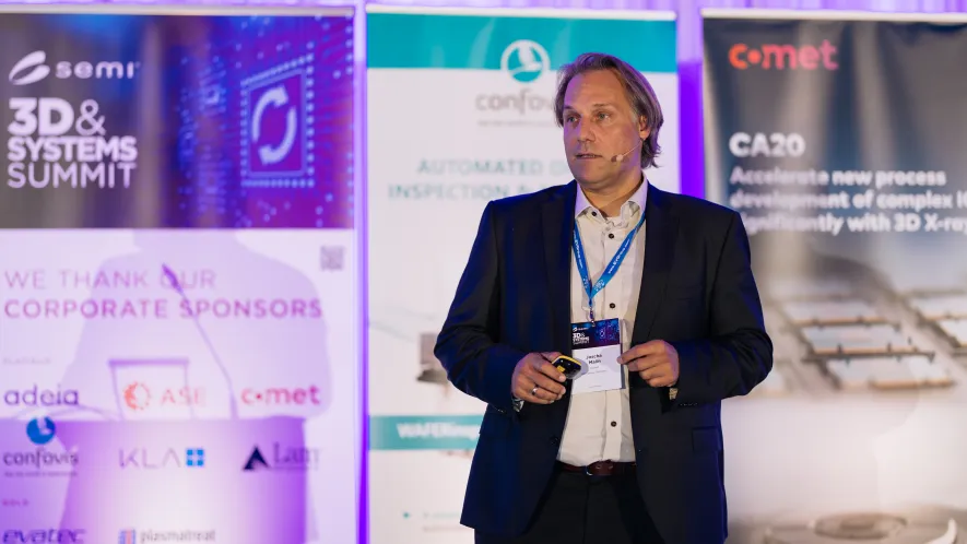
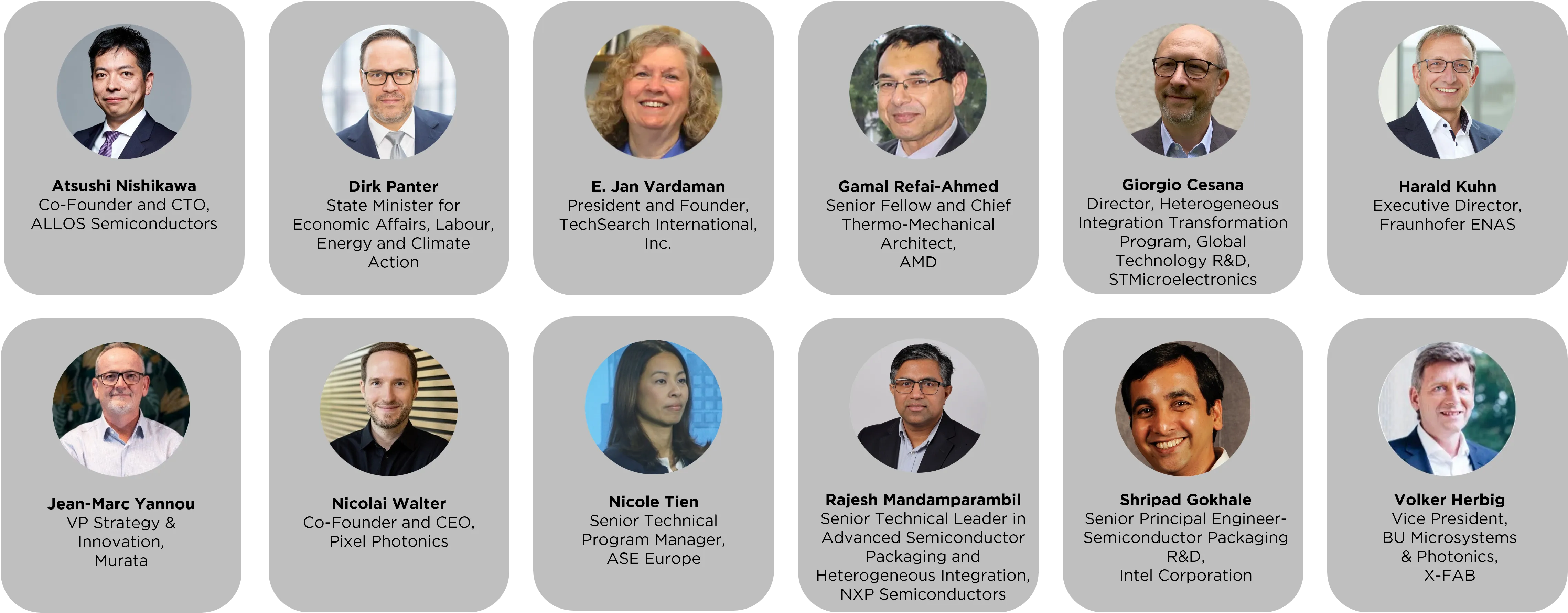
Featured Speakers
Enabling Next-Gen Heterogeneous Systems Integration
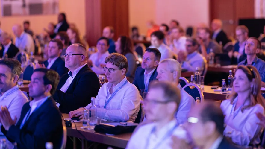
The SEMI 3D and Systems Summit brings together semiconductor packaging leaders to explore the strategies and technologies driving next-generation heterogeneous systems integration.
This year's theme, Enabling Next-Gen Heterogeneous Systems Integration, focuses on exploring geopolitical dynamics, market trends, strategies to advance Europe's next-gen semiconductor solutions, and the latest technological advancements.
Expert-led sessions cover chiplet architectures, hybrid bonding, co-packaged optics, AI-driven system architectures, AR/VR, and wearable intelligence, with a strong focus on Europe's role in advancing design leadership, materials innovation, and the transition from lab to fab.
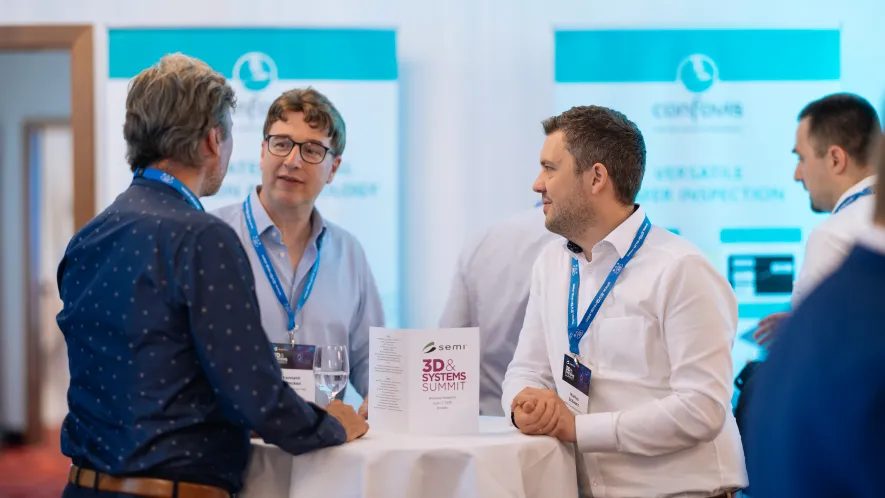
The exclusive exhibition area showcases industry leaders alongside innovative emerging companies, providing a platform for gathering and exchanging knowledge and foster collaborations.
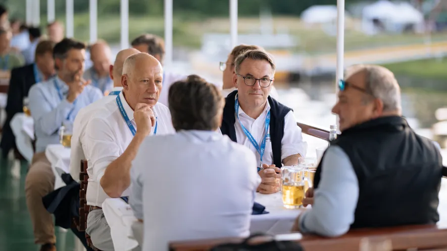
Attendees will have several opportunities for B2B matching, including networking receptions, coffee breaks, lunches, and a unique Networking Dinner Cruise along the beautiful Elbe River.
Sponsors
Platinum
Gold
Event
Agenda
Registration, Networking Reception and Exhibition

Thursday, June 18
Summit Opening

Opening Remarks
This session examines shifting geopolitical dynamics and their impact on semiconductor supply chains, industrial policy, and Europe’s long-term technological resilience. Speakers will address global benchmarking, fab construction updates, and regional strategies. Insights will highlight where Europe stands today and what actions are needed to secure technology sovereignty across critical domains.

Opening Remarks by Session Chair

Heterogeneous Integration as a Strategic Lever for Europe’s Semiconductor Resilience
From Chip to AI Factory: A Five-Year Roadmap for Silicon Suppliers and Hyperscalers

From Portfolio to Products: Unlocking Europe’s Potential with Heterogeneous Integration
Networking Coffee Break

A Geographical Assessment of the Advanced Packaging Market

Panel Discussion - European Infrastructure for Semiconductor Manufacturing: What’s Missing?
Biographies
Moderator
-E. Jan Vardaman
Panelists
-Rajesh Mandamparambil
-Gamal Refai-Ahmed
-Giorgio Cesana
Key Takeaways by Session Chair
Advanced packaging is central to enabling next-generation heterogeneous systems. This session spans fan-out packaging, OSAT strategies, supply chain considerations, and lab-to-fab technology transfer. Speakers will highlight European strengths, procurement challenges, and what is required to scale advanced packaging capacity regionally.

Opening Remarks by Session Chair

Primidi: A European 300 mm Fab Line OSAT serving Advanced Packaging Integration
Advanced Packaging at Scale: Bridging Innovation, Qualification, and High‑Volume Manufacturing

Scaling Advanced Packaging Inspection Through AI-Enhanced X-ray Analysis: Insights for Glass Panel Inspection

Advancing Redistribution Layer Plating for Enhanced Reliability and Performance
Networking Lunch
Advanced Panel Processing for Heterogeneous Integration on Large-Area Substrates

One Platform for Defect Inspection and 3D Metrology from Visible Light to Infrared
Lab-in-Fab: Accelerating 3D System Integration from RTO Research to Foundry High-Volume Manufacturing
Key Takeaways by Session Chair
Hybrid bonding is establishing itself as a cornerstone of high-density 3D integration. This session covers die-to-wafer and wafer-to-wafer bonding, DRAM stacking, reliability engineering, and integration challenges. Attendees will learn how hybrid bonding accelerates 3D architectures across memory, logic, and advanced packaging.
Opening Remarks by Session Chair

A New Era of Reworkable Hybrid Bonding

Process Control in W2W and D2W Hybrid Bonding

Implications of Hybrid Bonding on Lithography Alignment, Metrology, and Overlay Control
Key Takeaways by Session Chair
Networking Coffee Break
Co-packaged optics and photonic integration are key enablers of high-bandwidth communication, AI acceleration, and energy-efficient data movement. This session highlights European leaders in photonics, packaging, and quantum technologies. Speakers will address opportunities across optical interconnects, quantum photonics, and high-volume manufacturing.

Opening Remarks by Session Chair

Inside the Package: How CPO is Powering the Next Wave of AI

ARCTIC: Enabling Scalable Photonic Detection for Co-Packaged Optics

High Density TSV Silicon Interposers as an Enabling Platform for Optical Datacom

Scalable MicroLED Optical Link Prototype Fabrication for the Next Generation Computing

Heterogeneous integration, Key to High Frequency Integration

Low-Pressure Plasma Processes for Photonic Packaging and Co-Packaged Optics
Key Takeaways by Session Chair
Networking Dinner Cruise
The Networking Dinner Cruise is set on a historic paddle steamer on the Elbe River, just a 5-minute walk from the Hilton Dresden Hotel. Following the final conference session, attendees will gather in the hotel lobby and be escorted to the pier by the SEMI Europe team onsite.
Friday, June 19
AI computing demands breakthroughs in scale, power efficiency, and memory bandwidth. This session covers wafer-scale engines, European AI accelerators, integrated photonics, and power delivery for high-performance AI systems. It also examines how Europe can position itself in the next wave of AI hardware.

Silicon Capacitors: A Ubiquitous Enabler in Advanced 3D-Integrated Data Center Systems

Advanced Packaging for AI Era - Challenges and Opportunities with Heterogeneous Architectures
Autonomous Edge Chiplets: Building the Reference Platform for Scalable Edge Compute
Networking Coffee Break
Europe’s future competitiveness depends on strengthening semiconductor design capabilities. This session highlights chiplet architectures, CPU startups, 3D integration strategy, and the importance of building a strong design ecosystem. The speakers will present cutting-edge activities that position Europe as an emerging leader in system-level architectures.

Opening Remarks by Session Chair

GaN-on-Si Epiwafers with 200 and 300 mm Diameter are a Crucial High-Tech Material Enabling Breakthroughs for AI-Age Displays and AI Datacenter Infrastructure

Driving System Level Energy Efficiency in AI with Advanced Packaging and Heterogeneous Integration
Key Takeaways by Session Chair

Closing Remarks and End of 3D & Systems Summit
REGISTRATION

Delegate Ticket Prices:
- SEMI Members: 1,195 EUR *
- Non-members: 1,695 EUR *
Delegate Ticket Includes:
- Conference sessions and keynote presentations
- Exhibition access
- Coffee breaks and lunches
- Networking Reception (June 17)
- Networking Dinner Cruise (June 18)
Please note: The Networking Dinner Cruise is included for registered delegates unless stated otherwise.
Please note:
- All prices exclude statutory German VAT (19%)
- Prices exclude accommodation and transfers
Let Your Network Know You’re Attending the 3D & Systems Summit and Boost Your Visibility! Spread the word and make connections with industry leaders, innovators, and peers by sharing your participation on LinkedIn.
As a matter of fundamental principle, SEMI adheres to the highest level of ethical standards. Maintaining public trust is core to our being. SEMI embraces the law’s spirit to ensure our actions always align with the public expectations.
Accommodation
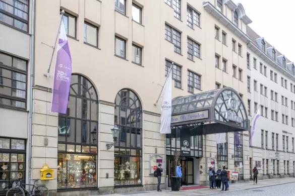
An der Frauenkirche, 5
D-01067 Dresden, Germany
Tel. 0049 (0)351 86420
- Room rate starts at 149 EUR per night
- Booked rooms are cancellable free of charge till 7 days prior to arrival
- For booking a room a guarantee by credit card is mandatory
- The offered room rate is including our Hilton Breakfast buffet, service charge, and VAT
Exhibition and Sponsorship
Become an Exhibitor
Booth Prices:
- SEMI member: 3,995 EUR*
- Non-SEMI member: 4,495 EUR*
* VAT excl.
Turnkey booth includes booth space & structure, furniture, electricity, and a delegate contingent. Arrive on-site, place your materials, and engage—additional equipment available for rental, including a presentation monitor on a stand. Prices in EUR (net), excl. 19% German VAT.
Contact: [email protected]
Become a Sponsor
Sponsorship of 3D & Systems Summit offers valuable opportunities to elevate your company's visibility through Thought Leadership, On-site Visibility, Strategic Networking, and Targeted Marketing. SEMI members receive a 10% discount on all sponsorships.
Make the most of your participation – whether as a sponsor or attendee – by utilizing the available resources. Access the digital library for event logos, PowerPoint templates, banners, and more to enhance your visibility before, during, and after the event. Let your LinkedIn network know you're attending the summit and share your participation here.
Contact: Salil Gupte at [email protected]
Event App
Plan Your 3D 2026 Experience.
- The event app allows you to:
- View the full session schedule
- Explore the speaker list
- Connect with other attendees
- Schedule 1:1 meetings in advance of and during the event
- Access your digital registration badge, which will be helpful during onsite check‑in at the venue
We recommend downloading the app ahead of the event so you can start planning your schedule and meetings in advance.
Partners
SEMI is proud to partner with the following media and associations to bring you news about this event. If you are interested in partnering with us, please contact: Sitong He at [email protected]
 |  | |||
 |  |  |  | |
 |  |  |
3D & Systems Summit Committee
The 3D & Systems Summit Committee engages in shaping the program of the event which addresses the most relevant and advanced topics related to the 3D packaging roadmap, Heterogeneous Integration and System-In-Package (SiP) manufacturing. Thank you to our Committee Members for making 3D & Systems Summit a success!
3D & Systems Summit 2026
June 12, 2026 - SEMI 3D & Systems Summit to Spotlight Heterogeneous Integration as Key to Europe's Semiconductor Future
3D & Systems Summit 2025
June 24, 2025 - SEMI 3D & Systems Summit and NextGen Talent Open Tomorrow to Spotlight Heterogeneous Integration for Europe’s Semiconductor Resilience
June 9, 2025 - SEMI 3D & Systems Summit to Highlight Heterogeneous Integration as Key to Europe’s Semiconductor Resilience
April 30, 2025 - SEMI 3D & Systems Summit to Spotlight Trends in Hybrid Bonding, Chiplet Architecture and Geopolitical Dynamics
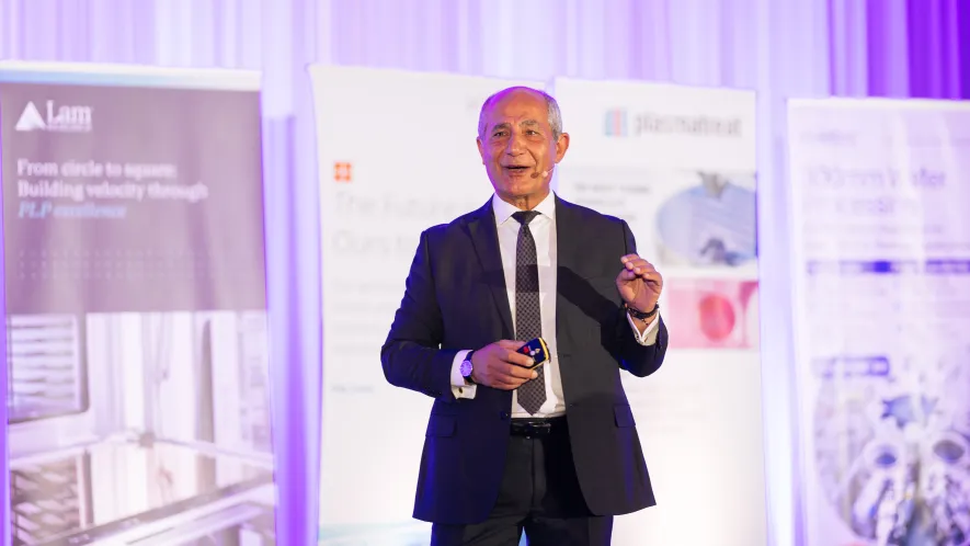
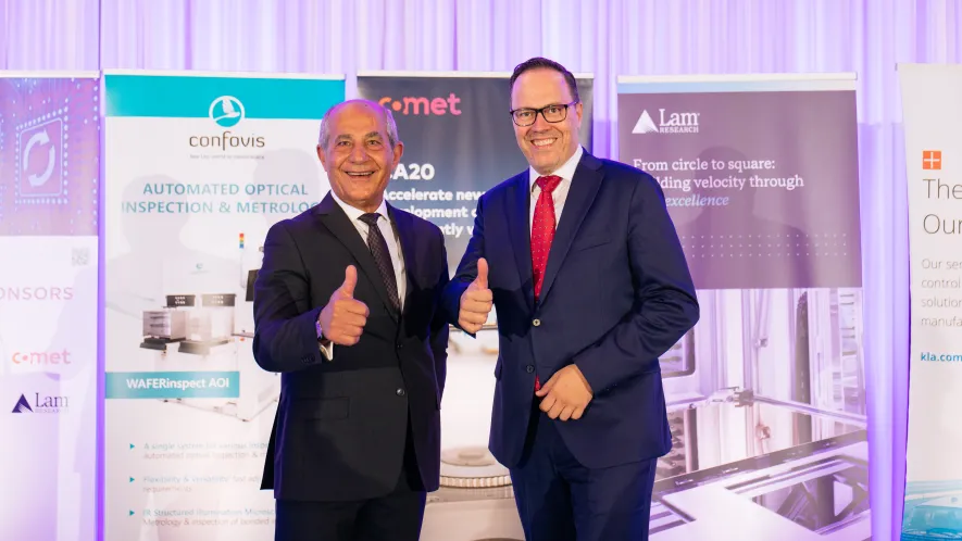
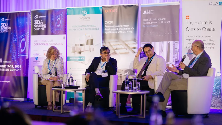
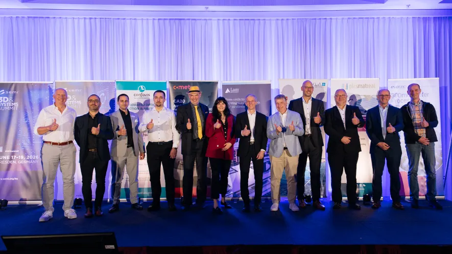
Photo Gallery