
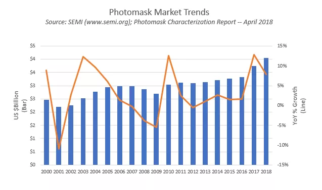
The semiconductor industry has been on a roll for the past few years – and the rising tide has lifted segments spanning the supply chain. The photomask market, in particular, has seen exceptionally strong growth of 13 percent and 8 percent in 2017 and 2018, respectively. The upsurge is striking given that, in the early to mid-2000s, the photomask market averaged less than 4 percent annual growth. And the gap between the past two years and the previous 10 (2006 to 2016) is remarkable. During that span, annual photomask market revenues hovered around $3 billion for a 10-year CAGR of a mere 1 percent.
What is driving this historically robust growth? Several factors, including the extension of 193nm immersion and other deep ultraviolet (DUV) lithography with multiple exposure/patterning technologies. All require multiple masks. What’s more, the Internet of Things (IoT) is sparking resurgent demand for older mask sets for 200mm fabs, a segment where merchant mask houses are well-positioned. And finally, but with less impact to growth, 2018 marked the introduction of long-delayed extreme ultraviolet (EUV) lithography into production by Samsung. TSMC implemented EUV lithography in its second generation 7nm devices earlier this year. Both companies will use EUV for their 5nm designs. Intel will insert EUV at their 7nm node, which is roughly equivalent to Samsung and TSMC’s 5nm node. And while current EUV mask volumes are nominal, their average selling prices are not.
Historically, EUV was viewed as a technology that had to be more cost effective than optical lithography before it could be introduced into production. The twist today is that as process complexity has increased, the promise of EUV to reduce mask counts, improve pattern fidelity, and consistently improve higher electrical yields, EUV has become more compelling. Despite the upsides, technology challenges such as EUV pellicle readiness, sub-optimal resists, and the lack of robust actinic inspection tools continue to hinder the mass roll-out of EUV technology.
 Last month, SEMI reported that the worldwide semiconductor photomask market logged a record high in 2018, reaching $4.0 billion. SEMI also noted that captive mask suppliers have significantly boosted their market share due to the increasing capital outlays required to make leading-edge masks since the turn of the century. However, merchant shops did manage to regain a percentage point from captives last year – captive shops claimed 64 percent of the market compared to 65 percent in 2017 largely because more advanced (sub-45nm) masks represented a larger portion of their total sales.
A recent SEMI published report, Photomask Characterization Summary, provides details on the 2018 Photomask Market for seven regions of world including North America, Japan, Europe, Taiwan, Korea, China, and Rest of World. The report also includes data for each of these regions from 2003 to 2020 and summarizes lithography developments over the past year.
Please click on the SEMI Photomask Market Characterization Executive Summary for a copy and on SEMI Market Information for information on the all the markets SEMI covers.
Lara Chamness is a senior market analyst, Industry Research and Statistics, at SEMI.