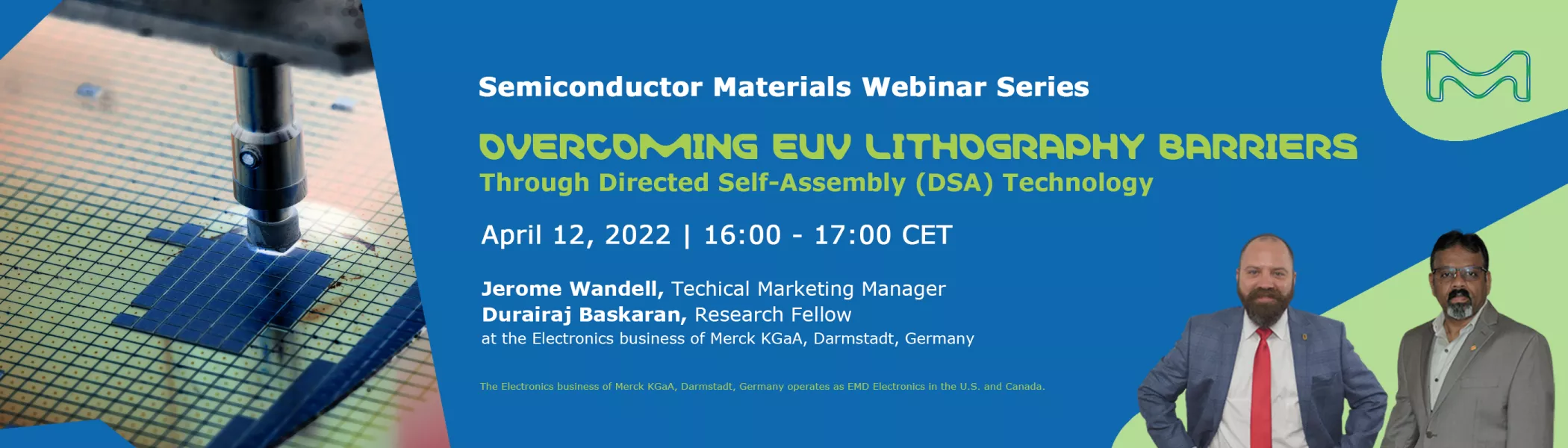
April 12, 2022
Sponsored by the Electronics business of Merck KGaA, Darmstadt, Germany.
Time
4:00 pm - 5:00 pm
Location
Online, Central European Time (CET)
Germany
This webinar is the third webinar in a series exploring pressing topics on materials and semiconductor development.
Join us to discover how Directed Self-Assembly (DSA) technology and its material development can help overcome the scaling barriers of EUV lithography. We will discuss how EUV tooling requires a radically different design resulting in a source photon deficiency of approximately 90% compared to its processor, 193nm immersion lithography. This source limitation leads to new scaling barriers, including:
- CD variance, or line-width roughness, is difficult to mitigate and has severe yield implications.
- Source power limitations have a direct effect on throughput, resulting in a productivity challenge.
- Market factors such as high-consumer demand for semiconductors combined with the DRAM supplier's imminent need for EUV tooling.
In this webinar, you will learn how Directed Self-Assembly (DSA) technology and its material development can solve many of these limitations. The complex molecular assembly of DSA will be explained, and we will walk through the steps of how it can be integrated into an advanced patterning process. In addition, the CD variance limitations of EUV will be compared to the variance derived from a DSA process, and we will evaluate its unique solution to accommodate the EUV photon limitation.
Why Attend?
Our Semiconductor Materials Series attract semiconductor industry professionals, business and technology leaders, researchers, academics, and industry analysts from across the electronics supply chain around the world.
Register today to access exclusive content during an interactive session.
You will be able to apply innovative techniques and best practices to solve your unique challenges. Live Q&A will follow.
Attendees are invited to submit questions ahead of time at info_semi_webinar@emdgroup.com.
Agenda

Welcome Remarks

Welcome Remarks by the Electronics business of Merck KGaA, Darmstadt, Germany

Biography
Jerome Wandell has spent 25 years working in semiconductor lithography, covering many aspects of the field, including process development, photoresist formulation chemistry, and design-to-mask (OPC). His current role is Technical Marketing Manager for the Directed Self-Assembly (DSA) materials portfolio of the Patterning Solutions group for the Electronics business of Merck KGaA, Darmstadt, Germany. Jerry received a bachelor's degree in Microelectronic Engineering from the Rochester Institute of Technology and is now based in Saratoga Springs, NY. His prior roles in lithography were at GLOBALFOUNDRIES, Rohm & Haas, and ASML.
Biography
Dr. Durairaj Baskaran is a Research Fellow in the Electronics business of Merck KGaA, Darmstadt, Germany. He develops materials for the directed self-assembly of block copolymers and selective monolayers for applications in advanced patterning. He has over 25 years of experience in designing macromolecules and taught "Organic Chemistry of Polymers" at the University of Tennessee for many years, before moving into industry.
He has published 100+ research articles in peer-reviewed international journals, edited a book, and filed several US and Indian patents. He has also directed industrial research projects from Solvay (Italy), P&G (US), GE (India), as well as obtained grants from the Office of Naval Research (Navy), NSF, and US army.
LIVE Q&A and Conclusions
- Q&A Moderated by Laith Altimime, President, SEMI Europe
- Conclusions by Anand Nambiar, Executive Vice President, Semiconductor Materials, the Electronics business of Merck KGaA, Darmstadt, Germany
REGISTRATION
Registration is FREE of charge. If you miss the live session, register for on-demand access.
The webinar is also available on LinkedIn Live where the attendees have the opportunity to network with other participants.
Our Semiconductor Materials Series audience of influencer business and technology leaders, executives, researchers, and industry analysts from across the electronics supply chain around the world.
JOB FUNCTION
• Business Development
• Chemicals/Materials
• Design
• Engineering
• Environment, Health and Safety
• Equipment
• Executive Management
• Fabrication and Process
• Facilities
• Field Service
• Government and Public Policy
• Manufacturing/Operations
• Packaging/Assembly
• Purchasing and Procurement
• Quality Assurance
• Research and Development
• Test
• Automotive Electronics
• Consumer Electronics
• Display
• Flexible Hybrid Electronics/Printed Electronics
• IoT
• Medical Electronics/MedTech
• MEMS/Sensors
• LED/Solid State Lighting
• Photonics
• Photovoltaic/Solar
• Semiconductor
• Software/Applications
Areas of Interest
A broad range of products and technologies from across the semiconductor supply chain, from design to manufacturing.
Products & Services
DESIGN/MANUFACTURING SERVICES
• Design/EDA
• Electronic Manufacturing Services (EMS)/System Integration
• Fabless
• Factory Control/Process Software
• Foundries
• Manufacturing Services and Consulting
• Packaging and Test Services (OSAT)
• R&D/Technology Transfer
MANUFACTURING EQUIPMENT
• Abatement/Environmental Systems
• Assembly/Packaging
• Components/Sub-systems/Instrumentation
• Factory Automation: Robotics
• Front-end Processing
• Inspection and Measurement/
Metrology
• Large-area/Thin Film
• Parts
• Printing/Coating/Roll-to-Roll
• Secondary Equipment and Services
• Test
MATERIALS
• Cleaning
• Consumables
• Inks/Pastes/Printing Materials
• Packaging/Assembly
• Process Materials: Gases/Liquids/Solids/Chemicals
• Wafers/Substrates
Sponsors