SEMI spoke with Balaji Nandhivaram Muthuraman, Package and Material Simulation engineer at Dialog Semiconductor, about the state of reliability testing for wafer-level chip scale packages ahead of his presentation at the Advanced Packaging Conference at SEMICON Europa 2018, 13-16, November 2018, in Munich, Germany. To register for the event, click here.
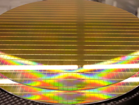
SEMI: Since the beginning of package development reliability testing has played a key role in Wafer Level Chips Scale package (WLCSP) investigation. Lately, the role of simulation and predictive reliability significantly contributed in reducing package development time. To what extend can we predict potential failures for WLCSP packages in an early design phase by simulation?
Muthuraman: Reliability testing is essential and crucial for the electronic packages. It is during the package development phase that several design iterations need to be considered and, in some cases, many feasibility studies for the package are executed. This means we require significant reliability test measurements, which could influence product-development time. For example, Temperature Cycling on Board (TCoB) reliability testing would take approximately 65-75 days for testing the package reliability subjected to 1500 temperature cycles. Each cycle involves exposing the device at hot and cold temperatures with a specified temperature profile.
Executing such Board Level Reliability (BLR) tests for all feasible package designs is a tedious process that could lead to an increase in package development time. This is the stage where numerical simulation methodology helps us to foresee potential failures in Board Level Reliability. Predicting delamination or cracking of passivation/metal interface layers based on the WLCSP design layout and estimating the characteristic life of smart device subjected to temperature load are some classic examples of predicting WLCSP package behavior in an early design phase by simulation methodology.
SEMI: We can definitely say that predictions occurring during the early stage are key to success. But how exactly can numerical simulation help estimating?
Muthuraman: From a thermal reliability point of view, determination of the optimum material combination – bill of materials for device – is used to predict whether a heat sink is required for the device to meet thermal performance. This is not all. At an early design stage, the simulation methodology can be used to estimate device performance under varying thermomechanical loads. Numerical simulation at early package development phase helps the researchers by predicting the possible temperature contour field and stress contour field of the smart device under a given loading condition.
The estimation accuracy of potential issues through numerical simulation depends on the material models implemented and consideration of realistic load condition under which the package operate in real life situation. For example, engineering judgements can be made using numerical simulation of Solder Joint Reliability (SJR) analysis to decide whether an Underfill material is required between the Package and the Printed Circuit Board (PCB).
SEMI: Are all conditions tested during the reliability investigations specific to fit a certain type of applications or do these vary?

Muthuraman: Reliability investigations are based on the end application of the electronic devices. For example, handheld device applications will be exposed to a reliability condition up to a maximum of +85oC, whereas smart devices designed for an automotive application would be tested with a typical temperature of +125 oC or up to +150 oC. In some cases, the testing conditions are customized based on specific customer requirements. Moreover, reliability conditions can also be customized to study some specific failure mechanism.
SEMI: Can you describe for which one?
Muthuraman: Thermal cycling profile is based on device application and/or specific requirement from our customer. For example, handheld devices use a typical temperature range of +85°C to -40°C with 20°C/min ramp time and 20 minutes of dwell time. There is possibility of adjusting the ramp and dwell time of the Temperature Cycling qualification test, provided such accelerated test does not lead to other failure modes.
SEMI: What failure mechanism was the subject of the study in this specific case?
Muthuraman: Electronic package reliability behavior without and with underfilled devices is explained in this study with the help of temperature cycling on board (TCoB) measurements and validated with numerical simulation. In the paper to be presented at SEMICON Europa, failure occurring at the interface of the solder and Under-Bump Metallization (UBM) structure is discussed. Behavior of such failure mechanism is illustrated with different WLCSP package sizes subjected to varying thermal load condition.
One of the key aspects of the subject is the board-level reliability (BLR) measurement and simulation validation showing how the failure mode could be shifted from solder joint to the metal interface layers between UBM and interconnection to Silicon Chip, depending on the WLCSP design layout. The reasons for such shifts in Failure phenomenon are explained and necessary design optimization is suggested for improvement. Another key aspect of this study is determination of Fatigue Life Model for WLCSP family using the SACQ solder.

SEMI: Are you currently working and experimenting on something particularly exciting?
Muthuraman: Recently, we concluded our engineering analysis of thermomechanical reliability of Large Wafer Level Chip Scale packages. In September 2018, I presented this research work in an International Conference held in Dresden, Germany. Dialog Semiconductor GmbH was awarded the “Best Paper Presentation for the year 2018” for this work. This success is attributed to the entire team of Package and Material simulation experts at Dialog Semiconductor GmbH lead by Mr. Baltazar Canete and IC Package-Design & Simulation group managed by Mr. Rajesh Aiyandra.
We have started our investigation on the influence of Board Level Reliability of WLCSPs due to varying metal concentration of inter-metallic layer. We, at Dialog, are also working on possibility of thinner WLCSP. All these activities would include extensive Temperature Cycling on Board (TCoB) measurements, Statistical Analysis of measurement Data and would then be validated by Numerical Simulation.
SEMI: What are your expectations for the future and why would you recommend attending SEMICON Europa Advance Packaging Conference?

Muthuraman: SEMICON Europa is an important platform for Dialog Semiconductor GmbH to showcase the latest developments in the semiconductor industry. It is an opportunity to meet other industry experts, partners, and customers, and exchange various innovative ideas and to get new insights. Many semiconductor companies are based around the Munich area as well world-class universities. We are particularly interested in innovation, workforce and talent development themes.
SEMICON Europa gives us a platform for greater interaction with the academicians and research scientists. This way, we bridge the gap between industry and University researches, thereby moving forward in innovative technologies. We, as Dialog Semiconductor GmbH, have also a development center near Munich (Germering). Our expectations for the future are very positive and vibrant. We are always ready to take up the industry challenges and demands and provide the best-in-class solutions to our product users. Dialog Semiconductor GmbH is certainly poised for higher growth in coming years.

Balaji Nandhivaram Muthuraman Bio
Balaji Nandhivaram Muthuraman is a Packaging and Material Simulation engineer at Dialog Semiconductor GmbH, Germany. He has authored/co-authored conference publications including in the area of molecular dynamics simulation on assembly of carbon nanostructures; Analysis of thermoset material used in smart devices and reliability of wafer level packages. Recently, he has been awarded with the “Best Paper Presentation for year 2018” in the area of Board Level Reliability of Wafer Level Chip Scale Packages, in a recently held international semiconductor conference. His current areas of working interest include reliability investigation of electronic packages and developing fatigue models for reliability assessment of Dialogs products. He obtained his Bachelor’s degree in Aeronautical Engineering from Anna University, India and Master’s degree in Computational Mechanics of Materials and Structures from University of Stuttgart, Germany.
Serena Brischetto is a marketing and communications manager at SEMI Europe.