Heterogeneous integration involves the assembly of separately manufactured components and requires the combination of a broad variety of different materials with diverse physical characteristics. Redistribution layers (RDLs) consisting of copper conductor lines and organic dielectric are key to connecting functional components of a number of technologies. In order to improve the reliability of this assembly, the mechanical properties of the individual materials need to be optimized. Chemistry solutions that satisfied reliability requirements of the past are no longer enough to meet the challenges presented by decreased miniaturization and More than Moore. What new chemistry solutions are needed and how will they enable the industry to extend the More than Moore roadmap?
SEMI spoke with Markus Hörburger, global product manager, Atotech Deutschland GmbH, about Atotech’s holistic approach to improving the reliability of advanced heterogeneous packaging through innovative chemistry solutions for fan-out wafer-level packaging (FOWLP) in 5G applications. Hörburger shared his views ahead of his presentation at the SEMI Advanced Packaging Conference at SEMICON Europa, 12-15 November, 2019, in Munich, Germany. Join us at the event to meet leading experts from Atotech and thought leaders from the global advanced packaging community. Registration is open.
SEMI: Various materials come into play in heterogeneous integration of different components. What are the primary challenges of this complexity to performance reliability?
Hörburger: Combining various materials with different physical characteristics, such as thermal expansion, strains the materials during assembly and operation, impacting the reliability of the entire package. In order to overcome this issue, the mechanical properties of the individual materials need to be optimized. However, shrinking dimensions in next-generation packages limits the ability to optimize these properties. For example, fan-out wafer-level packaging (FOWLP) – whose redistribution layers (RDL) consist of copper (Cu) traces and organic dielectrics – decreases Cu traces and the opportunity to optimize it properties. Therefore, we need a new approach that focuses not on the optimization of individual materials, but also takes into account surrounding materials within the package.
SEMI: What key factors influence the optimization of the mechanical properties?
Hörburger: In a package, thermal expansion is mainly dominated by die and mold, which creates high strain on thin Cu traces. A high material ductility helps offset the strain by allowing significant plastic deformation before rupture. A high Cu purity improves ductility since Cu impurities usually accumulate in grain boundaries, increase embrittlement and result in intergranular fractures when exposed to thermal lead. However, this individual purity optimization is only one option for decreasing Cu traces.
SEMI: How is performance reliability affected if these factors are not controlled?
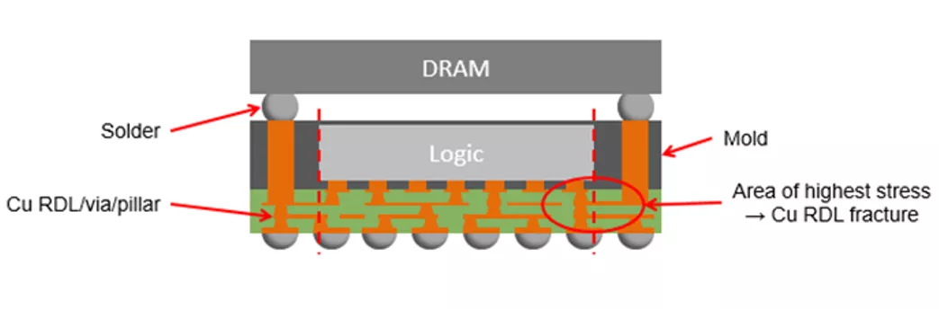
Hörburger: It is proven that for high strains, only ductile materials show improved reliability. That means if the copper redistribution layers (Cu RDL) do not show a sufficient ductility, the thermal expansion mismatch between RDL and adjacent dielectric may result in fractures. For fan-out wafer-level packaging, the fine Cu RDL lines that are closed to transition from die to mold become increasingly susceptible to fracture, risking a significant yield reduction in the case of unreliable Cu traces.
Heterogeneous Packaging
Risk from shrinking RDL dimensions
SEMI: How does Atotech’s new chemistry solution overcome these challenges and what led to these advancements?
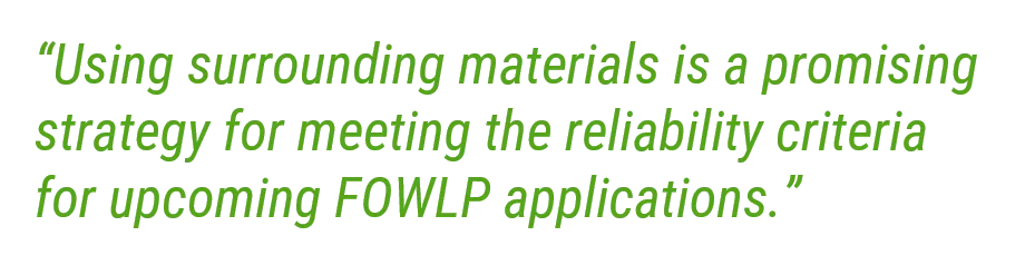
Hörburger: A chemical solution based on special additive design can help optimize the reliability of Cu RDLs. But overcoming the limitation of individual components for small Cu lines requires a holistic approach. Atotech focuses on composite formation between Cu RDL and adjacent dielectrics to create a strong interconnection between individual components with beneficial synergetic effects. Using the surrounding materials is a promising strategy for meeting the reliability criteria for upcoming FOWLP applications.
 One way to achieve a strong adhesion between Cu RDL and dielectric is to create a rough Cu surface. However, due to high frequencies and the resulting skin effect, adhesion based on rough Cu is not suitable for 5G applications. In order to offer a solution for 5G applications, the adhesion mechanism must also be effective for smooth surfaces.
Atotech’s custom-designed chemistry solutions result in high-purity Cu deposits, excellent adhesion to dielectric, the highest reliability due to purity and strong composite formation and smooth traces. All of these attributes lend themselves to 5G applications.
SEMI: Considering the limitations of existing chemistry solutions, the potential for this holistic approach seems promising beyond 5G applications. What other applications would this new solution benefit?
Hörburger: The holistic chemical approach would benefit all package technologies with shrinking dimensions heterogeneously integrated into one package. Potential applications are AI, high-performance computing and autonomous driving, where high reliability and yield are key criteria.
SEMI: What are your expectations for the Advanced Packaging Conference at SEMICON Europa 2019 in Munich?
Hörburger: The Advanced Packaging Conference is a key packaging platform in Europe where international experts present and discuss major trends and solutions. This is a great opportunity to exchange innovative ideas across the entire supply chain. For Atotech and other chemical suppliers, it is important to understand future requirements in order to provide excellent chemistry solutions for advanced packaging technologies.
 Markus Hörburger joined Atotech in 2014 as a product manager and is in charge of plating chemistries for Semiconductor Advanced Packaging, Leadframes and Connectors. Prior to Atotech, he built an Innovation Network at BASF in his role as strategic project manager. Hörburger received his degree in business chemistry from the University of Ulm.
We thank Ralf Schmidt, R&D manager, Semiconductor, at Atotech Group for his valuable scientific contribution.
Serena Brischetto is senior manager, marketing and communications, at SEMI Europe.