19 New Fabs to Start Construction
Equipment spending rises by 1.5% in 2016 and 13% in 2017
By Christian G. Dieseldorff, Industry Research & Statistics Group at SEMI (June 8, 2016)
The latest update of SEMI’s World Fab Forecast report reveals that 19 new fabs and lines will begin construction in 2016 and 2017. Fab equipment spending was off to a sluggish start in 2016 but is gaining momentum for a projected 1.5 percent year-over-year growth by the end of the year, followed by a projected 13 percent growth in 2017.
Fab equipment spending including new, secondary, and in-house declined by 2 percent in 2015. Activity in the 3D NAND, 10nm Logic, and Foundry segments is expected to push equipment spending up to US$36 billion in 2016, 1.5 percent over 2015, and to $40.7 billion in 2017, up 13 percent. Equipment will go into existing fabs and lines that are being converted to leading-edge technology and also into new fabs and lines that began construction in the prior year.
Table 1 shows the regions where new fabs and lines will be built this year and next. These are projects with a probability of 60 percent or higher, according to SEMI’s data. While some are already underway, others may be subject to delays or pushed into the following year. The SEMI World Fab Forecast report, published May 31, 2016, provides more details about this construction boom.
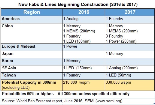
Breaking down the 19 projects by wafer size, 12 of the fabs and lines are for 300mm (12-inch), four for 200mm, and three LED fabs (one each for 150mm, 100mm, and 50mm). Not including LEDs, the potential installed capacity of all these fabs and lines is estimated at almost 210,000 wafer starts per month (in 300mm equivalents) for fabs beginning construction in 2016 and 330,000 wafer starts per month (in 300mm equivalents) for fabs beginning construction in 2017.
In addition to announced and planned new fabs and lines, SEMI’s World Fab Forecast provides information about existing fabs and lines with associated construction spending, e.g. when a cleanroom is converted to a larger wafer size or a different product type.
Table 2 lists all construction projects — including new and ongoing — planned for 2016 and 2017, by wafer size, with total estimated spending of $14 billion.
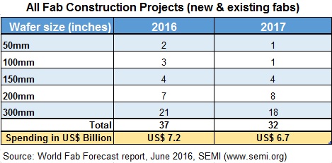
Examining fab construction projects by wafer size reveals which product segments are responsible for this growth. 100mm and 50mm projects, over both years, are all for LED production. 150mm wafer projects will supply Analog, Foundry, MEMS, and LED needs. For 200mm wafers, in 2016, Analog and Power dominate, while in 2017, Power takes the lead. 300mm wafers are mainly for Memory and Foundry, with some Analog, Logic (MPU), and Power.
In addition, the transition to leading-edge technologies (as we see in planar technologies, but also in 3D technologies) creates a reduction in installed capacity within existing fabs. To compensate for this reduction, more conversion of older fabs may take place but also more new fabs and lines may begin construction.
To learn how semiconductor manufacturing will look in 2016 and 2017 and details about capex for construction projects, fab equipping, technology levels, and products, visit the Fab Database webpage and order the SEMI World Fab Forecast Report. The report, in Excel format, tracks spending and capacities for over 1,100 facilities including over 60 future facilities, across industry segments from Analog, Power, Logic, MPU, Memory, and Foundry to MEMS and LEDs facilities. Using a bottoms-up approach methodology, the SEMI Fab Forecast provides high-level summaries and graphs, and in-depth analyses of capital expenditures, capacities, technology and products by fab.
The SEMI Worldwide Semiconductor Equipment Market Subscription (WWSEMS) data tracks only new equipment for fabs and test and assembly and packaging houses. The SEMI World Fab Forecast and its related Fab Database reports track any equipment needed to ramp fabs, upgrade technology nodes, and expand or change wafer size, including new equipment, used equipment, or in-house equipment. Also check out the Opto/LED Fab Forecast. Learn more about the SEMI fab databases at: http://www.semi.org/en/MarketInfo/FabDatabase and www.youtube.com/user/SEMImktstats
Related: Highlights of the May 2016 Edition of the Fab Databases
Follow SEMI on LinkedIn and Twitter.
Global Update
SEMI
www.semi.org
San Jose, California
June 8, 2016