200mm Fab Investment Finds Home in China
By Clark Tseng, Industry Research & Statistics Group, SEMI
China’s ambitious plans to build a world-class semiconductor manufacturing supply chain domestically certainly has the industry’s attention. With over a dozen new 300mm fab announcements lately from Foundries, DRAM, 3D NAND, and as well as CMOS image sensor companies (either from international semiconductor makers or from indigenous players), China has launched a huge investment in wafer fab capacity that is expected to ramp in the next five years.
While advanced 300mm fab investment attracts most of the attention and resources, China does not skimp on the more “matured” 200mm fabs. China will have the most new 200mm fab projects and capacity additions in the next few years compared to other regions. According to SEMI’s latest 200mm Fab Outlook report, China currently has about 700,000 wafers per month (wpm) installed fab capacity, and this is forecasted to surpass 900,000 wpm by the end of 2021, or over 28 percent growth in five years. By then, China’s 200mm capacity is expected to surpass America, Japan, and Taiwan, and be second only to Europe.
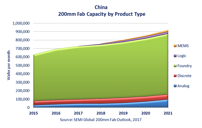
A further examination of China’s new 200mm fab projects shows a wide diversity in products. Beyond the usual 200mm foundry investment led by SMIC and Hua Hong Semiconductor, an increasing number of new projects are focusing on analog, power, and MEMS applications. According to SEMI’s latest 200mm fab Outlook report, China will add eight new 200mm volume fabs between 2016-2021: two for foundries, two for analog, two for MEMS, one for power, and one for logic.
In the meantime, China is not limiting itself to adding wafer capacity. It is also developing material and equipment capabilities around 200mm wafer manufacturing. A number of silicon wafer suppliers are emerging in China targeting 200mm and smaller wafer markets. On the equipment side, the 200mm tool availability remains the biggest challenge for the industry in adding more 200mm capacity; some projects have been postponed because of it. China equipment suppliers are expected to take the opportunity to develop the tool sets needed to satisfy the upcoming demand for these fabs.
China’s 200mm capacity will evolve to make more than “legacy” products, e.g., smart card, Analog IC, and Discrete IC. These manufacturers will become more versatile advancing into MCU, PMIC, CIS, fingerprints sensor, power, MEMS, and other devices. With the rise of China’s electronic OEMs and automakers, these 200mm fabs will play an even more important role supporting various manufacturing ecosystems in China.
For more information, visit https://discover.semi.org/global-200mm-fab-outlook-registration.html.
Global Update
SEMI
www.semi.org
July 5, 2017