
2020 was a year that made a mark in the history of mankind as well as the semiconductor industry. It was a year of business and personal disruptions caused by COVID-19, supply chain interruptions, and exceptional agility of industries coping with the new normal imposed by the pandemic. Nevertheless, it was a year of extraordinary growth for the semiconductor industry, including semiconductor manufacturing materials.
The global semiconductor materials market registered continuous growth in recent years and has annually exceeded $50 billion since 2018. The market expansion was driven by chip shipments increases as well as the advanced process requirements in both wafer fab and packaging segments. In 2020, the global semiconductor materials market expanded 5% to reach $55.3 billion in revenue to set a new industry record. The momentum in growth is expected to continue throughout 2021 despite the lingering pandemic.
The main drivers of the continued upward trends are the increased digitization of global economies, the deployment of 5G technologies, and robust investments in data centers and cloud services. Manufacturing of advanced node ICs, 3D memory architectures, and heterogeneous integration require more processing steps and, as a result, drive higher wafer fabrication and packaging materials consumption.
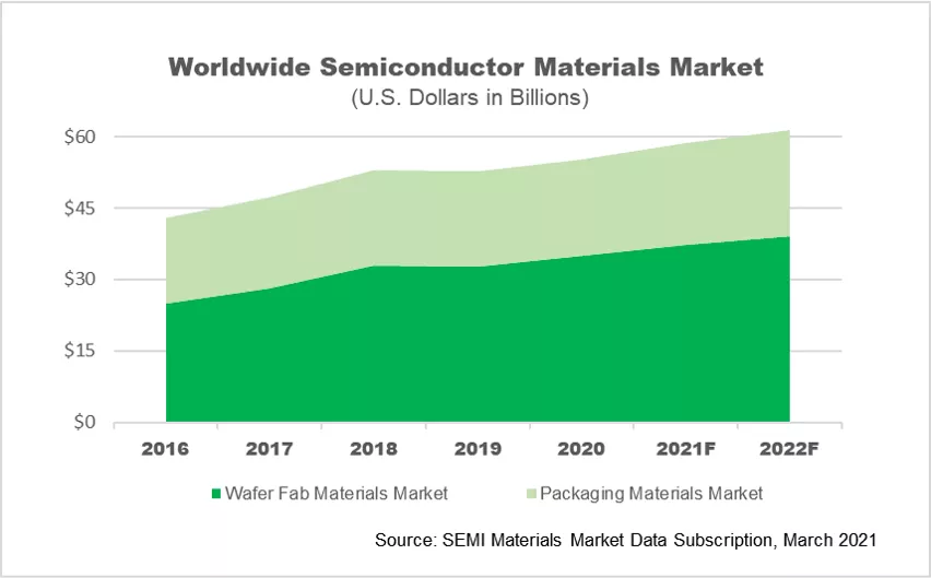
In 2020, wafer fabrication materials revenues increased 6.5% to $34.9 billion. Among major wafer fab materials, photoresist and photoresist ancillaries, wet chemicals and CMP (slurries and pads) saw the strongest growth.
Within the photoresist category, the lion’s share is attributed to advanced photoresists that exhibited 22% growth in 2020. The continued quest for scaling drives the need for advanced lithography technologies and, as such, expanding the use of EUV and multi-patterning of critical layers to spur higher consumption of 193nm and 13.5nm photoresists. EUV, in particular, is rapidly being deployed in high-volume manufacturing for leading-edge logic devices with over 85 tools installed and running production by the end of 2020.
The volume of CMP and wet chemicals required to support the increasing number of processing steps, paired with the cost of advanced formulations of CMP used for leading edge technology manufacturing, contributes to the expansion of the CMP and wet chemicals markets. In 2020, these segments recorded 15% and 17% growth, respectively.
Overall, 2020 represented record spending in all wafer fab materials categories except sputtering targets and silicon. The silicon wafer market has been cyclical in the past and is typically sensitive to supply and demand dynamics. In 2020 silicon wafer shipments grew 5% over 2019, however silicon market revenue remained flat from 2019 due to soft pricing in the first half of 2020. With strong 300mm epitaxy wafer demand and improved growth in 200mm and 300mm polished wafers, the silicon wafer market is poised to rebound strongly in 2021.
The packaging materials market increased 2.3% to $20.4 billion in 2020. As for specific materials, organic substrates remains the largest packaging materials segment. The strength of the substrate market is driven by the adoption of high-performance computing and 5G. However, the current supply tightness could adversely impact the growth potential for various applications.
Wirebonding materials saw a rebound in demand in 2020 driven by consumer electronics, laptops, and other work-from-home and learn-from-home related applications. Recent wirebonding capacity builds by OSATs to meet increased demand should enable this growth to continue. The leadframes market in 2020 remained at the level of 2019 because of a weak first half of 2020 due to the disruptions caused by the pandemic, especially from the automotive sector. Powered by a strong rebound starting at the end of 2020, the automotive sector will contribute to the leadframes market expansion in 2021. Other materials in the packaging segment, like ceramic packages and encapsulation resins, also saw a soft 2020 but should edge up in 2021.
From a regional perspective, Taiwan remained the world's largest consumer of semiconductor materials for more than a decade. Aggressive capacity ramps in China have elevated the region to become the second largest market of materials in 2020. Korea ranked third among top regions. A similar regional profile is also expected in the coming years based on the strength of Taiwan’s large foundry capacity and advanced packaging base, massive government investments in China, and the strength of memory production in Korea. While recent trade and geopolitical tensions and export restrictions may contribute to supply chain and regulatory uncertainties, the overall technology sector is strong and poised for long-term growth, which should be reflected in significant investments for semiconductor materials.
In any case, the COVID-19 pandemic has accelerated the digital transformation of many business and that has, in turn, dramatically increased consumption of semiconductor content to the benefit of the entire semiconductor manufacturing ecosystem. While keeping the uncertainty of geopolitical trade tensions and overall macroeconomic factors in mind, the semiconductor materials market was strong in 2020 and is positioned for healthy growth ahead as we adjust to a new post-pandemic normal.
For more information about semiconductor materials market trends by region and segment, please see the SEMI Materials Market Data Subscription (MMDS).
Inna Skvortsova is a market analyst in Industry Research and Statistics at SEMI.