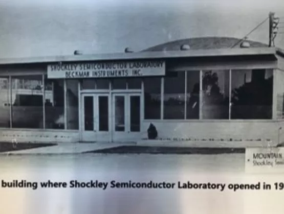
Adapted from the Computer History Museum’s “Celebrating the Birthplace of Silicon Valley” invitation.
Work that sowed the seeds of the digital, hyper-connected world we know today all started in a squat, unremarkable building in Mountain View, California. Long before the structure’s foundation was laid, Santa Clara County flourished with orchards, not chips. Between the 1880s and 1940s, eight million fruit trees carpeted Silicon Valley. By 1939, San Jose, with a population of 57,651, was the largest canning and dried-fruit packing center in the world, with 18 canneries, 13 dried-fruit packing houses, and 12 fresh-fruit and vegetable shipping firms*.
In 1956, silicon sprouted from new fertile ground.
That’s when startup Shockley Semiconductor Laboratory, employing some of the most brilliant young minds in the business, produced Northern California’s first silicon transistor prototypes and formed the technological and cultural bedrock for today’s Silicon Valley.

Fed up with William Shockley’s hard-nosed management style, eight Shockley employees – including Gordon Moore, Robert Noyce, Julius Blank, Victor Grinich, Jean Hoerni, Eugene Kleiner, Jay Last, and Sheldon Roberts – resigned in September 1957 and founded Fairchild Semiconductor Corporation. Fairchild was the seedling from which companies valued at over $2 trillion have grown and the source of the integrated circuit “computer chip” that has revolutionized our world.
Now, more than 60 years later, the site of Shockley Labs, already an IEEE Historical Milestone, is being formally recognized by the IEEE and the City of Mountain View for its historical significance in a special dedication ceremony on August 15. Thanks to the efforts of many, especially developer Merlone Geier Partners, newly commissioned public sculptures – in the likeness of two early semiconductor devices and a mammoth silicon crystal monument that symbolize the work to come out of the lab – now permanently mark the site, along with various plaques that describe and commemorate the site’s history.

The event’s featured speaker is Professor James F. Gibbons, former dean of engineering at Stanford University. Professor Gibbons’ first task at Stanford in 1957 was to work with Shockley and his team to transfer their knowledge of silicon fabrication to Stanford, which could in turn train future engineers for the coming boom in the semiconductor industry. He will share his personal experiences and memories of those early days.

Join early semiconductor pioneers, the president of the IEEE, SEMI president and CEO Ajit Manocha and local officials on August 15 to commemorate this legendary Silicon Valley landmark. Guests are invited to enjoy a series of presentations and exhibits and view the stunning sculptures and plaques.
The event is free to attend and open to the public. Space is limited so please sign up here to guarantee a seat.
Location: 391 San Antonio Road, Palo Alto, California (Phase II of San Antonio Village). Parking is free.
*National Park Service, Santa Clara County: California’s Historic Silicon Valley
Ariana Raftopoulos is a marketing manager at SEMI.