Semiconductor foundries have their shoulders to the wheel of the Fourth Industrial Revolution, and nearly 60% have reportedly embarked on their own digital transformation journey. However, of the advanced industry cohort of WEF’s Global Lighthouse Network, electronics, electrical components, and automotive manufacturers boast 22 beacons collectively – the avant-garde in the successful adoption of Industry 4.0 technologies. Fabs number only three.
The findings of a 2021 Mckinsey & Company study point to the source of a missed opportunity for the chip sector — Artificial intelligence (AI). The study concludes that AI can potentially deliver the semiconductor industry operational gains of $85-$95 billion annually in earnings before interest by 2025. In reality, roughly 90% of this figure remains theoretical.
With this context in mind, it’s natural for innovative semiconductor veterans to pursue the value of AI. Markus Keil, Vice President of Global Operations at Optotune, is among them. Keil has long sought new opportunities for semiconductor process engineers to level up their standard operating procedures to reduce fabrication costs. Twenty years back, he presided over a critical technological step change involving Advanced Process Control (APC).
 “We measured the remaining thickness of the Interlayer Dielectric and metal layer post-chemical mechanical planarization (p-CMP), using that to adjust the recipe polish time to meet the right target,” Keil explained. “For this, multiple thickness points (and hence uniformity) were measured on several wafers per batch. The approach was ultimately implemented as a fully integrated and automated system between deposition and CMP to adjust recipes on both tools. Similar logic has since been used for years for etch-litho to adjust critical dimensions (CD) after exposure and etch. In this context, APC can be considered a predecessor to AI/ML.”
Here, a successful APC experiment was established as a state-of-the-art practice on millions of wafers and is, these days, “old technology” for a chip processing sub-step.
In 2023, Keil sees fabs as an obvious target industry for the machine learning megatrend, appreciating that mature AI has the capacity to outperform APC while addressing the semiconductor industry’s perceived data overload and digital maturity issues:
“Daily discussions with customers are about data quality and availability. Millions of data points come in daily from several hundred pieces of equipment,” Keil said. “So fabs often struggle to gain access to the right data. Then it’s a question of whether to trust it and how to interpret and leverage the data for value. Data scientists can collaborate with process engineers and use AI to narrow the mass of data to a handful of critical parameters. This is where I think machine learning is so powerful.”
Machine Learning Value Drivers

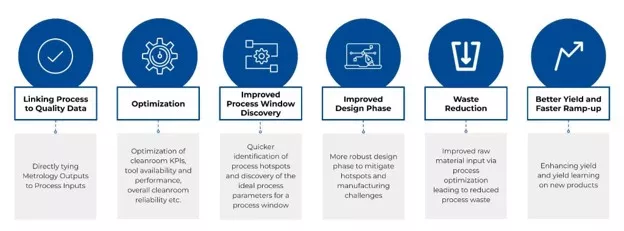
AI-driven solutions leverage process and quality data. For this reason, they can be deployed to optimize semiconductor fabrication and design holistically.
Smart factory initiatives embed a data-to-value workflow. Deep learning algorithms can then generate insights into the complexities of the physical production process. However, as stated in a white paper from the WEF with the Boston Consulting Group, Data Excellence: Transforming Manufacturing and Supply Systems, digital capacity building lends itself to a cross-disciplinary partnership model with humans in the loop.
A case in point, Benny Leonard, CTO at DataProphet, is a senior data scientist specializing in solving optimization problems with AI models he builds from scratch with his teams in diverse manufacturing environments. Leonard stresses the importance of collaborative push-pull between industrial AI practitioners and functional manufacturing experts.
“Data scientists are good at interpreting numbers from the data domain,” Leonard noted. “But for machine learning models to be effective, they need a good understanding of what they are modeling.”
Before data can be a source of truth, AI algorithms need to be rigorously interrogated for validity.
“Because numbers don’t talk to you, experts in the field may initially see AI as a black box, giving instructions without justification,” Leonard elaborated. “Machine learning prescriptions can be hard for manufacturers to trust. But healthy skepticism is good. Someone with 30 years of manufacturing experience must be confident an AI model will guide a process they know intimately in an even better direction, especially if it’s counterintuitive. I welcome interaction with our customers. It helps us understand their process better.”
Leonard’s team recently completed a successful AI-driven etch map prediction project with a semiconductor manufacturer that also designs and builds processing systems.
In the targeted substep, the tool etches silicon wafers by illuminating them with ion beams through a grid to produce a specific thickness profile. Multiple process variables in exposing the (mostly rotating) wafer for etching include the etch time duration, the angle of the wafer with respect to the grid, and the beam power. Existing manufacturing specifications limit grid assembly deviations, ensuring etched wafers fall within acceptable tolerances. However, dispersion via the grid is complex and non-linear. Grid measurements can, therefore, be technically within specifications but produce etch profiles of poor quality.
“Because an existing baseline model vouched for the grid’s quality even if defective, we developed a machine learning model to take grid measurements as input, predicting whether the resulting wafers would meet quality standards,” Leonard explained. “Predictions of non-quality meant the grid needed to be re-assembled or scrapped.”
What are the implications of this work for semiconductor manufacturers?

By feeding the input parameters during the multiple etching steps into a supervised deep-learning model, the team achieved something unprecedented. As Leonard put it:
“We predicted deformities in the shape of the chip post etching within the order of six angstroms — this metric constituted extreme accuracy compared to the previous benchmark.”
Consider that there were 13 input channels and that a channel was a set of anything from 500 to 2,400 data points. It is beyond the scope of human capacity to factor in these variables (linear and nonlinear) to accurately predict the chip uniformity after etching. And yet, framing the post-etch defect metric as an image problem, the customer could view the entire chip radially out from the center at any given location — based purely on the input parameters.
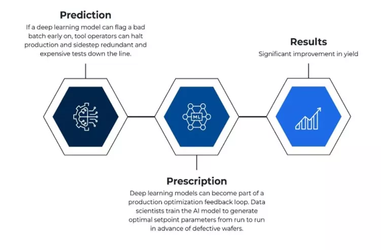
To remain competitive into the next decade, silicon players must scale technological force multipliers. The rewards of AI for their bottom line are within reach. Prescriptive AI prevents defective chips and determines the path of more quality wafers — drawing predominantly on historical data to significantly improve yield with minimal CapEx.
Nicol Ritchie is in marketing at DataProphet.