
Prior to 1997, the industry enjoyed the “mask maker’s holiday” when IC feature sizes were larger than the lithography wavelength and the industry enjoyed the number of transistors per area doubling for no additional cost. This era ended when 248nm lithography was adopted. 248nm lithography enabled device manufacturers to extend traditional optical lithography but forced the adoption of resolution enhancement techniques such optical proximity correction and phase shift masks. 193nm lithography was introduced for 90nm features and the industry was required to adopt increasingly complex strategies to shrink device geometries further such as liquid immersion, double patterning, and more recently multiple patterning. These techniques have enabled device manufacturers to extend traditional optical lithography while next-generation lithography approaches, including extreme ultraviolet (EUV), maskless lithography, and nanoimprint remain in the background.
EUV is the most favored next-generation lithography and has received the lion’s share of press and research dollars. EUV was initially scheduled to be used for 65nm feature processing but persistent challenges with this technology remain unsolved. Key obstacles associated with EUV are: finding adequate source power, EUV photoresists, and developing mask manufacturing infrastructure. Significant progress has been made and there are now beta EUV tools in the field. The extended delay of EUV forced chipmakers to extend 193nm immersion lithography with multiple patterning down to sub-10nm. With so much invested in optical lithography, even when EUV is ready, it is expected that chip makers will use a combination of EUV and 193nm immersion with multi-patterning for leading-edge devices.
The delay in EUV for volume production has impacted the photomask market. Last month, SEMI reported that the worldwide semiconductor photomask market recorded a record high in 2016, reaching $3.32 billion. SEMI also noted that captive mask suppliers have significantly increased their market share due to the capital intensity required by leading-edge manufacturing.
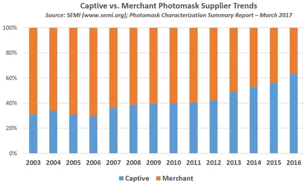
It remains to be seen what lithography solutions the industry will implement to maintain Moore’s law as the costs of advanced lithography increase faster than increased device density gains. What is clear is that the photomask market is mature and that captive shops, with their deep pockets, are assuming an increasingly important role. Still merchant shops continue to serve a vital function by servicing standard mask sets and providing manufacturing capability in the event of a service disruption.
A recent SEMI published report, Photomask Characterization Summary, provides details on the 2016 Photomask Market for seven regions of world including North America, Japan, Europe, Taiwan, Korea, China, and Rest of World. The report also includes data for each of these regions from 2003 to 2018 and summarizes lithography developments over the past year.
Please click here to download a copy of the SEMI Photomask Market Characterization Executive Summary. For information on all SEMI Market Information, visit: www.semi.org/en/MarketInfo.