
Introduction
Automated production in electronics manufacturing can produce high-quality products, but it might lead to a particular failure without human interventions. With the rapid technology development, such as the Industrial Internet of Things (IIoT), big data analysis, cloud computing, artificial intelligence (AI), many manufacturing processes can be more intelligent, and Industry 4.0 can then be realized in the near future[1]. Smart manufacturing adopts real-time decision-making based on operational and inspectional data and integrates the entire manufacturing process as a unified framework. Then, the future manufacturing process transforms cyber-physical systems digitally and responds to any uncertain situations proactively while ensuring higher efficiency.
In Surface Mount Assembly (SMA) lines, equipment status and quality data can be collected via IIoT technology. Data-driven solutions, such as AI and machine learning algorithms, can be applied to diagnose abnormal defects and adjust optimal machine parameters in response to unexpected changes/situations during production. Collaborating with various SMT industry partners, the research team at the State University of New York at Binghamton (aka Binghamton University) developed a novel framework based on AI-based closed-loop feedback control and parameter optimization to implement a smart manufacturing solution in the PCB assembly for yield and throughput improvement. This AI-based framework could provide a potential road map for data-driven process control in SMA.
Machine Intelligence in SMA
Each SMA process has a critical effect on the final PCB product quality and throughput. Notably, the solder printing process is a critical operation because over 60% of the PCB assembly soldering defects can be traced back to this stage. An inadequate volume of solder paste transferred to any PCB pad is a printing fault, which leads to board failure and substantial reworking and repair costs. The pick and place (P&P) process is the highest cost procedure, including expensive machine investment and extended production time. In the soldering reflow process (SRP), the reflow oven temperature and other related settings determine the solder joints' quality and reliability. Hence, multiple inspection machines in the SMA processes have been introduced, including solder paste inspection (SPI) and automated optical inspection (AOI) machines. Particularly, two independent AOIs could be employed to detect the components' defects before and after SRP.
Because many electronics components become small-scale (e.g., ), more assembly-related failures are often observed in recent SMA processes. The Smart Electronics Manufacturing Laboratory (SEML) at Binghamton University is fully equipped with two solder paste printers, two chip-mounters, and a reflow oven along with SPI and AOI machines. The research team tested more than 8,000 PCB at SEML. The results show that numerical methods based only on physical properties might have practical limitations in explaining small-scale components' behavioral patterns. It might be caused by unknown environmental factors (e.g., temperature and humidity), machine calibration, measurement accuracies, vibrations, etc., which could have influenced the quality of the SMA outcomes. However, recent research shows that AI-based methods can increase product quality up to 35%, reduce scrap rates, and optimize fab operations in semiconductor manufacturing, compared to traditional approaches[2]. It implies that a data-driven intelligent SMA process control has the potential to advance SMA processes.
The goal of the smart SMA is to maintain optimized settings in both offline and online scenarios. The AI and data analytics solution can optimize all SMA process parameters before production (i.e., offline control) and during production (i.e., online control). The overall schematic of the AI-based closed-loop feedback control framework is illustrated in Figure 2.
Intelligent SMA Modules
In the solder printing process, four machine intelligence modules are considered:
- Printing advising module (PAM)
- Printing optimization module (POM)
- Printing diagnosis module (PDM)
- Dynamic stencil cleaning process control (CPC)
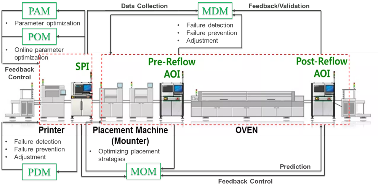
Figure 2. A schematic diagram of the AI-based closed-loop feedback platform
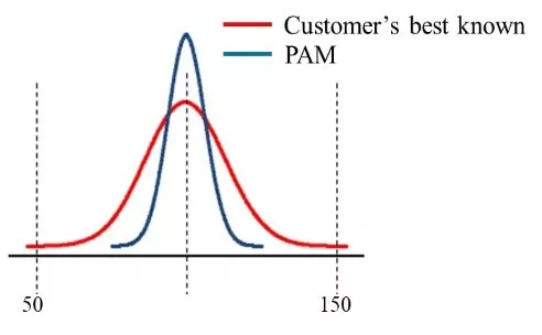
Figure 3. PAM effectiveness over customer’s best-known printing parameter setting
PAM aims to recommend the ideal initial setting of the printer critical parameters, such as printing speed, printing pressure, and separation speed, using hybrid machine learning and heuristics optimization techniques[3]. As a case study, the research team validated the PAM's performance with an automotive PCB testbed and compared the printing results to the best-known printing parameters. The experimental results show that PAM can achieve over 50% higher Cpk (i.e., process capability index, as shown in Figure 3).
POM optimizes printing parameters in real-time by monitoring printing quality and fine-tuning offset and process parameters for adapting to dynamic conditions[4]. The experimental results show that POM achieves more than 30% production quality improvement in terms of the Cpk by adjusting printing parameters compared to the offline control. PDM provides anomaly detection and diagnosis of the potential printing failure cases to improve process quality and reduce downtime[5]. The experimental results show that the PDM can achieve more than 87% accuracy in predicting different types of defects, improper printer hardware issues in the board support, squeegee, paste conditions, etc. The CPC uses the SPI information to estimate residue buildup level on the stencil undersurface and assess the stencil cleaning profile and cycle control, as illustrated in Figure 4[6]. Upon the implementation of CPC, it is expected that the robustness of the printing quality and the Cpk can be improved by 34% and 10%, respectively, compared to the best-known cleaning parameters using in the production line.
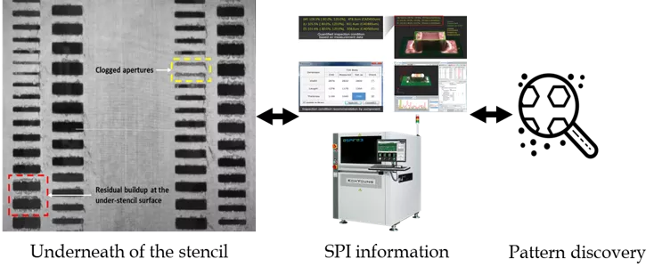
Figure 4. Smart residue buildup prediction for stencil cleaning operation control
During the P&P procedure, the mounter optimization module (MOM) and the mounter diagnosis module (MDM) can be applied as a machine's automation process while optimizing the P&P machine's parameters. By utilizing self-alignment effects appropriately, MOM identifies the optimal placement position by predicting the component's post-reflow positions based on the data collected by SPI, Pre-AOI, and Post-AOI machines, as shown in Figure 2. MOM also offers the placement positions adaptively during active production. In the MOM framework, multiple dynamic placement options are first generated based on the solder paste offset information. The components' final offsets in both x and y directions are predicted by a hybrid AI model that stacks on the k-nearest neighbor regression and the gradient boosting regression models. The optimal placement, which has the minimum predicted post-reflow misalignment, can be identified by MOM.
The experimental results show that MOM can decrease 18% of the final misalignments compared to a conventional P&P placement method (i.e., placing a component on the pad center). MDM is a prescriptive and predictive maintenance method that uses P&P machine operational and AOI inspection data to trace back the root causes of P&P defects and prevent future failure. MDM can achieve an accuracy of 84.50% in identifying the known root causes of certain defects, such as improper nozzle size, parts' contamination, and feeder problem. It shows that different mounting defects can be detected and classified automatically when the abnormality is detected through AI-based diagnosis algorithms.
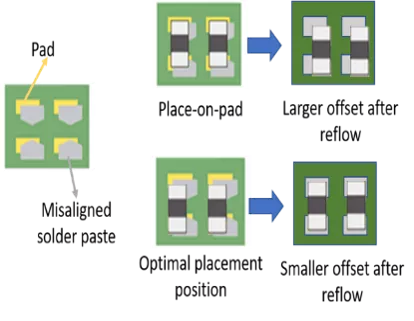
Figure 5. The illustration of the optimal placement position in the MOM
One of the reflow oven issues to be addressed is to find the optimal reflow oven temperature settings, which would affect the final quality of the PCB products. Solder paste manufacturers usually provide a target profile based on the solder paste composition's physical properties, and solder joint temperature is required to meet the given profile. Hence, reflow engineers should fine-tune reflow oven temperature manually to ensure a thermal profile outcome from the reflow oven to correctly meet a target profile, requiring substantial cost and effort. The research team proposes an automated reflow recipe optimization model based on the PCB thermal profile and its recipe.
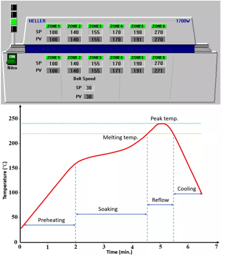
Figure 6. Optimized thermal recipe and thermal profile
First, the initial recipe collects the data for the prediction model and identifies the relationship between the thermal profile and the corresponding recipe. Then, an AI-based model is developed to predict the thermal profile based on the input recipe. Compared to traditional methods, the AI-based method generates an optimal reflow oven recipe to minimize the gap between the predicted temperature and the given profile. As a result, the AI-based prediction model allows us to achieve promising results, such as 97% of fitness in the given profile temperature curve within one hour of processing time. The proposed model has other significant advantages, such as saving time, labor, and materials. It enhances the degree of automation of the PCB reflow process. In the future, data from multiple inspection machines will be integrated so that the reflow optimization process is fully automated and generates more reliable results.
Summary and Conclusion
The small-scale electronics products make the SMA processes much more complicated to maintain high-quality PCB products, and theoretical interpretations of the SMA processes can be challenging due to many uncertain factors. With the help of AI and big data collected from various inspectional operations, SMA processes can be intelligent and flexible in response to dynamic environmental situations. While retaining the optimal control parameters throughout the SMA processes, the final PCB product quality can be enhanced while maintaining the designed throughput. Automated and smart systems bring about the opportunity to next level of electronics manufacturing, which utilizes the data and information from the end-users through edge/cloud computing and fastens the customized product manufacturing with increasing efficiency for high-mix/low-volume manufacturing. Also, it can increase verities of design and fasten the delivery time.
About the Author
 Prof. Sang Won Yoon is a recipient of the SUNY Chancellor’s Award for Excellence in Scholarship and Creative Activities in 2019 and a highly successful researcher who leads many productive long-term industry collaborations. Prof. Yoon received his doctoral degree in School of Industrial Engineering at Purdue University, and he joined the faculty of the Watson School in the Department of Systems Science and Industrial Engineering at State University of New York at Binghamton in 2010. Prof. Yoon has been studying how to extract useful insights from expanding data sets to support intelligent decision-making processes.
His research not only resides in better understanding large-scale data set by using statistical learning methodologies, but also leverages optimization, soft computing, simulation, and complex theories with conventional machine learning algorithms. As a result, Prof. Yoon has published in over 130 internationally renowned journals and conference proceedings. He was also a member of the Data Science Transdisciplinary Area of Excellence (TAE) initiative and is an active member of the Health Sciences TAE at his institution.
The author recognizes the following for their assistance with this article:
- Daehan Won, dhwon@binghamton.edu, Assistant professor
- Jingxi He, jhe56@binghamton.edu, Ph.D. candidate
- Shrouq M. Alelaumi, salelau1@binghamton.edu, Ph.D. candidate
- Yuanyuan Li, yli352@binghamton.edu, Ph.D. candidate
- Yuqiao Cen, ycen2@binghamton.edu, Ph.D. candidate
References
[1] Qi, Q., and Tao, F., 2018. Digital twin and big data towards smart manufacturing and industry 4.0: 360 degree comparison. IEEE Access, 6, pp.3585-3593.
[2] 10 Ways machine learning is revolutionizing manufacturing in 2019. https://www.forbes.com/sites/louiscolumbus/2019/08/11/10-ways-machine-learning-is-revolutionizing-manufacturing-in-2019/?sh=7cd2e9e22b40.
[3] Khader, N. and Yoon, S.W., 2018. Stencil printing process optimization to control solder paste volume transfer efficiency. IEEE Transactions on Components, Packaging and Manufacturing Technology, 8(9), pp.1686-1694.
[4] Lu, H., Wang, H., Yoon, S.W. and Won, D., 2019. Real-Time stencil printing optimization using a hybrid multi-layer online sequential extreme learning and evolutionary search approach. IEEE Transactions on Components, Packaging and Manufacturing Technology, 9(12), pp.2490-2498.
[5] Alelaumi, S., Wang, H., Lu, H. and Yoon, S.W., 2020. A Predictive Abnormality Detection Model Using Ensemble Learning in Stencil Printing Process. IEEE Transactions on Components, Packaging and Manufacturing Technology, 10(9), pp.1560-1568.
[6] Alelaumi, S., Khader, N., He, J., Lam, S. and Yoon, S.W., 2021. Residue buildup predictive modeling for stencil cleaning profile decision-making using recurrent neural network. Robotics and Computer-Integrated Manufacturing, 68, p.102041.