Air pollution is one of the grand challenges facing the entire planet — from the wealthiest nations to the least developed. The World Health Organization reports that nine out of 10 people breathe air containing high levels of pollutants, and that polluted air takes over seven million lives annually through stroke, heart disease and respiratory ailments.
As a result, the world is thirsty for reliable, high-performing chemical and environmental sensors that can provide previously unavailable real-time awareness of environmental conditions. On one level, this seems like a relatively simple step, given that smartphones are already equipped with miniaturized sensing technologies that can monitor our living environment and activities.
While highly desirable, embedding air pollution sensors in common mobile and wearable devices has not been feasible previously because the necessary trade-offs between high performance and miniaturization have made it impossible.
This situation drove a CEA-Leti team to develop a novel generation of fully integrated optical chemical sensors that leverage MEMS technologies. The team successfully merged multiple functionalities on the same chip, using integrated optics and photonics, fluidics, acoustics and electromechanical transduction. How did the team overcome significant technical obstacles to design a proof-of-concept device that senses multiple environmental pollutants — housed in a minimal hardware footprint?
Advancing Chemical Sensor Capabilities with Silicon
Featuring high selectivity, real-time performance, and fully reversible capabilities, optical chemical sensors are perfect candidates for industrial, environmental and biomedical applications. Consequently, in recent years, worldwide R&D initiatives have invested substantial effort to improve them.
R&D programs have focused particularly on the mid-infrared (Mid-IR) wavelength range (2.5 - 12 µm) — also known as the molecule fingerprint region, which provides a unique combination of fundamental absorption order-of-magnitude bands and unambiguous identification of specific chemicals. A multitude of molecules generate strong and distinct absorption lines in the Mid-IR, providing a foundation for accurate spectroscopic detection. Traditionally, however, these sensors have required large and expensive lenses for infrared (IR) light, making them too big and costly for resource-constrained wearables and mobile devices.

Fortunately, recent advances in integrated silicon photonics and quantum cascade laser (QCL) technologies have spurred investigation of new chemical sensor architectures. Richard Soref, a research professor at the University of Massachusetts Boston’s department of engineering, introduced the extension of Near-IR technology into the longer-wave Mid-IR infrared region in 2006. Soref’s concept showed that highly sensitive and selective gas sensors could be fabricated on planar substrates at low cost by co-integrating silicon MEMS, group IV photonics, and specifically designed III-V hetero-structures.
While this approach showed promise, it preceded the widespread availability of most mobile devices and wearables. Foreseeing today’s proliferation of those devices, CEA-Leti developed the different building blocks required to implement these concepts in real devices.
A New Concept of Integrated Optics
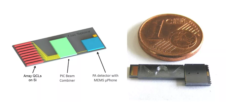
Leveraging these interesting findings, the institute developed a new combination of integrated optics and multiple sensor functions on a single chip: QCL sources, a photo-acoustic (PA) cell, and a mid-IR photonic integrated circuit (PIC) combiner. Their integration on a planar substrate (Figure 1) helped to achieve higher performance, new capabilities, and higher reliability at lower cost, all in a smaller package (less than a 1 cm3 or smaller than a 1-cent coin) with reduced weight and power consumption (less than 100 mJ per measurement).
 Figure 1: Fully integrated optical sensor (Courtesy: CEA Leti)
This configuration represents a multi-gas-detection enabler. The PIC replaces costly, fragile discrete optics while the PA detector uses a MEMS microphone to replace bulky multi-pass cells.
PA spectroscopy is among the most sensitive techniques available for monitoring chemical emissions or detecting gas traces. It relies on excitation of the chemical with a pulsed light source emitting at the absorption wavelengths of such molecules. The relaxation process creates local periodic variations of the temperature, resulting in stationary pressure waves, which high-performance microphones can detect.
 This new generation of devices, fully fabricated on silicon, shows performance comparable with state-of-the-art systems, with the huge bonus of small size and power efficiency that work well for mobile and wearable electronics. By supporting integration onto common technological platforms, such as on-chip photoacoustic sensors, researchers have successfully realized these miniaturized and cost-effective Mid-IR photonic devices in silicon. Mobile device and wearables manufacturers can now take advantage of manufacturable integrated devices for applications that are highly sensitive to size, performance and cost. Adding gas sensing to mobile devices and wearables is now very feasible.
For more information on chemical sensing at CEA-Leti, please visit or contact: http://www.leti-cea.com/cea-tech/leti/english
CEA-Leti is an active member of SEMI-MEMS & Sensors Industry Group. The technology research institute, along with Fraunhofer and imec, recently joined SEMI’s family as a Strategic Association Partner under a memorandum of understanding (MOU). Under this agreement, CEA-Leti will work with SEMI to advance technology roadmaps, industry standards and cutting-edge technologies including Internet of Things (IoT), artificial intelligence (AI) and machine learning that enable new capabilities across healthcare, automotive and other electronics manufacturing ecosystems.

 Sergio Nicoletti has more than 20 years of experience in micro and nanofabrication, including magnetic, superconducting and chemical sensing devices and technologies. Having joined CEA-Leti in 2006 as project manager for optical sensing devices used in chemical detection, Nicoletti is currently business development manager at the institute.
Previous positions include research and project management at CNR-IMM (Bologna, Italy) and at Hitachi Global Storage Technologies. Nicoletti was also a visiting scientist at HGST (San Jose, Calif.), where he worked on magnetic recording-head devices.
Nicoletti holds more than 20 patents and has more than 70 publications in peer-reviewed journals. In 2016, he was appointed coordinator of the European H2020 project MIRPHAB and is director of the project’s pilot line.
Nicoletti received his Ph.D. in physics, with a focus on HTc superconducting devices, from Université Joseph Fourier (Grenoble, France).
References
“Photoacoustic cell on silicon for mid-infrared QCL-based spectroscopic analysis,” JG Coutard, A Glière, JM Fedeli, O Lartigue, J Skubich, G Aoust, A Teulle, T Strahl, S Nicoletti, M Carras, L Duraffourg. Proceedings Volume 10931, MOEMS and Miniaturized Systems XVIII; 109310V (2019) https://doi.org/10.1117/12.2506514
“Miniaturization of mid-IR sensors on Si: challenges and perspectives,” S Nicoletti, JM Fédéli, M Fournier, P Labeye, P Barritault, A Marchant, A Glière, A Teulle, J Coutard, L Duraffourg - Silicon Proceedings Volume 10923, Silicon Photonics XIV; 109230H (2019) https://doi.org/10.1117/12.2506759