
May 29, 2024
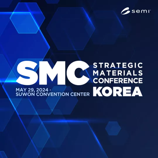
Materials Resilience: Navigating Challenges, Embracing Opportunities
Currently, sustainablility and efficiency of global supply chains are becoming more critical to the semiconductor industry. Global political tensions are affecting the semiconductor market, which is further revealing the vulnerabilities of the supply chain. In addition, ongoing environmental regulations are also having an increasing impact on the industry. The growing demand for eco-friendly products and manufacturing processes puts companies under pressure to introduce innovative technologies and solutions along with this regulatory compliance.
These trends present new challenges and opportunities for the semiconductor industry. SMC Korea reflects these issues and discusses current market conditions and future prospects. Through this conference, we expect major companies and experts will be able to share their experiences and knowledge, find innovative solutions together, and explore the future of the industry together. Don't miss these up-to-date discussions presented by global experts.
Time
10:00 am - 6:30 pm
Location
Convention Hall 2, 3F, Suwon Convention Center
Suwon-si
Gyeonggi-do
South Korea
OVERVIEW
- Date: May 29(Wed), 2024
- Time: 09:00 - 18:30
- Venue: Convention Hall 2, 3F, Suwon Convention Center
NOTICE
- Simultaneous interpretation will be provided
- Presentation files agreed by speakers will be provided to attendees.
SPONSORS
 |  |  |  |
 |  |  |  |
 |  |  |
CONTACT
- SEMI Korea Program Team (koreaprograms@semi.org)
Agenda
Welcome

Process Technologies for Continuous Scaling of Logic Devices
The rapid growth of AI, big data, IoT, and 5/6G communication necessitates the sophisticated computing power and efficiency of semiconductor devices, driving demand for various components such as HPC, GPU, ASIC, FPGA, and HBM. Semiconductor device and equipment industries are also challenging various new technologies to accommodate such diversifying applications and proceed with sustainable development in the era of AI and ICT.
According to the roadmap over the next 10 years, semiconductor technologies are expected to develop into the scaling technologies to further extend the existing Moore's Law and hybrid device technologies that integrate legacy nodes and advanced nodes into one. Therefore, in this presentation, we will look at the latest logic technology roadmap and introduce new process technologies to implement it.


Localization Challenges of the Materials Supply Chain

Material Trends in Advanced Packaging & Power Module Packaging (video recording)
Lunch

Materials Innovation Advancing the Angstrom Era
Materials innovation within the Semiconductor industry has been a driving force since the planar 2D MOSFET to the current 3D gate-all-around (GAA) transistor architectures and will continue its criticality as we embark on 500-layer flash memory designs and Angstrom level critical interconnect dimensions. To achieve these once incomprehensible levels of lateral and vertical scaling, device design engineers and manufacturers are increasingly relying on disruptive materials innovation to enable the density and performance gains required at each successive technology node. As the performance requirements for the most advanced devices become more challenging, materials have shown to have an increased contribution to device performance over scaling and design. This has led to a greater portion of the periodic table being incorporated into semiconductor processing.
The integration of new materials, such as novel photoresists, interconnect metals & alloys, ultra-pure polymers, chemically modified polymer membranes, and formulated chemicals, into the chip fabrication increases process complexity and makes yield ramps more challenging. With more process steps in the overall device build, speed to yield and process integrity are more critical than ever to achieve technology qualification schedules. This presentation will focus on Entegris’ approach to materials innovation, the integration of these novel materials coupled with co-optimized solutions enabling industry technology roadmaps and yield requirements while preserving integrity of delivery and process control.

Advanced Packaging Materials and Evaluation Platform at Resonac
Resonac has started Packaging Solution Center as new R&D center to propose one-stop solution for customers in 2018 and established the co-creative packaging evaluation platform “JOINT2” with leading companies to accelerate the development of advanced materials, equipment and substrates for 2.xD and 3D package in October, 2021.
2.xD and 3D packages require to connect chips and components in high density, therefore, both wiring pitch and vertical interconnect dimension must be finer and finer. At the same time, in order to achieve better performance, more and more chips are integrated together and thus the package size is increasing. To meet these requirement, we are developing fine vertical/lateral interconnect technology and the study of fabrication and reliability for the extremely large 2.5D advanced package.
The presentation will cover the significance and strengths of JOINT2, and updates on research and development.

Dry Resist for Holistic EUV Patterning
EUV lithography infrastructure has become the critical element of semiconductor industry to enable the device scaling down. It consists of not only light source, optical system but also masks, photoresist. The EUV stochastic effects present challenges to optimizing EUV resist resolution, line edge roughness, and sensitivity simultaneously. To overcome these challenges, Lam introduced the new dry resist combined with the new dry development technology.
Lam’s EUV dry resist, coupled with ASML’s EUV scanners and Lam’s holistic patterning solutions, will extend the patterning roadmap (Moore’s Law) for the next 10 years and beyond by offering a high-resolution, high-fidelity, defectivity-free, and greener solution for ≤32nm pitch L/S, and ≤40nm pitch pillar and contact hole EUV patterning in the fab. EUV dry resist technology also has been validated demonstrating superior dose-to-defectivity for <32nm pitch L/S, well suited for logic applications. Lam’s EUV dry resist is uniquely suited for future HiNA EUV patterning thanks to robust resist thickness scaling while maintaining high etch selectivity and high contrast.
Break
Sustainability Challenges of the Semiconductor Industry
Trends in Regulation of PFASs (per- and polyfluoroalkyl substances) and Technological Development Strategies
Fluorine compounds exhibit exceptional physical properties that set them apart from other organic materials. Consequently, they have been utilized as core materials to enhance the functionality, performance, and value of products across various key industries including electrical and electronics, semiconductors, displays, and automobiles.
However, on March 22nd of last year, the European Chemicals Agency (ECHA) issued a report imposing restrictions on the usage of over 10,000 types of per- and polyfluoroalkyl substances (PFASs) across all industries, sparking significant upheaval within the sector.
In this presentation, we will learn in detail about the definition of PFAS, and the content, progress, and schedule of PFAS regulations in Europe and the United States, and contemplate the direction of future technology development.

Sustainability Opportunities for A Diverse and Secure Fluorinated Material Supply Chain

Safer and Sustainable by Design: Strategies and Demonstration of PFAS Reduction in Photolithography Materials
Growing scientific evidences suggest that certain per- and polyfluoroalkyl substances (PFAS) pose global environmental and health risks. In response, global governments are contemplating measures to limit the use of these chemicals in various industries. However, specific types of PFAS are indispensable and no substitutes are currently available for most chip manufacturing applications in the semiconductor industry. Aligned with the objective of Safer and Sustainable by Design, DuPont has launched a comprehensive program to reduce PFAS usage in photoresist and associated lithography materials. In this presentation, we will provide an overview of DuPont's innovative initiatives and technical challenges encountered in this endeavor.

CORBION: PURASOLV® ELECT for a more Sustainable Semiconductor Manufacturing
Solvents are used extensively in the semiconductor manufacturing process. Solvents are estimated to be responsible for around 7% of the Scope 3 emissions of the semiconductor industry. The typical solvents that are used are produced from fossil resources and with that not in line with net zero ambitions. For more than 20 years Corbion has been supplying biobased ethyl lactate to the semiconductor industry under it’s brand name PURASOLV® ELECT, meeting the stringent requirements of the industry. Typical applications are photoresist for i/g-line / KrF / ArF / EUV, RRC, Edge bead removal and as thinner. Biobased ethyl lactate is sustainable and safe by design: it is produced from renewable resources, non-toxic and safe to workers, biodegradable and offers a significant carbon footprint reduction compared to incumbent solvents. Switching to biobased ethyl lactate thus enables more sustainable semiconductor manufacturing.
Break

Technology and Future of Semiconductor Packaging Materials
The technological advancement of semiconductor materials is a key factor along with the technological advancement of the process. And recently, the importance of Advanced PKG is increasing, and SK Hynix has achieved the result of improving product performance by developing MR-MUF materials. This proves the importance of materials. In the future, there are more packaging challenges for high-speed memory products such as HBM, and I plan to announce Need for material development to satisfy them.

Big Challenges for Small Worlds
The number of transistors in semiconductor chip has been increased twice every two years for more than 50 years, following the famous Moore’s Law and somehow, it was taken to be granted. In reality, it was a big accomplishment with an unimaginable amount of efforts and collaborations, including the development of new materials.
New material has been developed and introduced to improve the performance and capacity of electronic devices through smaller design rules. New Photo Resists (PR) for higher resolution with smaller defects and higher uniformity were developed. And Precursors were also developed to meet the process challenges for the smaller design rules, such as higher aspect ratios. High etch selective Etchant and CMP Slurry with low scratch were requested. And the requirements in new materials are getting tougher and stronger with the evolution of AI, which needs more computing power than ever. Even materials that has never been expected in industry and has been studied only in academia are being actively considered.
Even the worse, the surrounding situation for material development and manufacturing is getting tougher. Environmental regulations are getting tighter. Gases with high global warming potential were begun to be replaced. Recently, EU announced banning PFAS materials in near future and US raised bars for PFAS materials. And carbon zero policy is coming to us slowly but firmly.
In this talk, we will discuss the current status and future direction of material research. We will discuss the development directions to improve the performance of devices and to consider environmental regulations. And we will discuss the virtue of working together as a big one-team to overcome all the obstacles mentioned above in the world of extreme technology.
Networking Reception
Registration

Early-bird Registration Close: Wednesday, May 22(KST)
[Early Bird]
· SEMI Member: KRW 308,000
· Non-Member: KRW 363,000
[Regular]
· SEMI Member: KRW 385,000
· Non-Member: KRW 385,000
※ Registration fee includes lunch and reception.