A Communication Problem
As the industry ventures towards a more connected world, the semiconductor test community is facing increasingly stringent performance, quality and reliability targets, particularly in the high-stakes automotive, communications, and medical sectors. It is, therefore, important for device makers to know how their components will perform before their products hit the road, reach for the skies, or get placed inside the body. Access to test data is critical to mitigating failure risks. Yet many challenges are associated with accessing test and manufacturing data.
One hurdle is that component suppliers are often reluctant to provide test data for fear of revealing sensitive information about their design and/or manufacturing IP. With customers sourcing their components from multiple vendors, IP leakage is a valid concern and, consequently, a barrier to access. Certainly, these issues can be negotiated contractually, but only after striking the delicate balance between access and cost.
Beyond access, the quality of test data itself – which can be fragmented and even corrupted – is not always assured. As a device moves through the typical product flow (i.e., fab to sort to assembly to test), it inevitably changes hands (e.g., from foundry to OSATs). As a result, information about the device can become a patchwork of data where formats vary and certain fields, at times, may get overwritten. These potential gaps in test data flow underscore the need for consistent communications of manufacturing information from one process or stakeholder to the next. While standardization could help, it is currently lacking in many of these critical data-flow chains in the manufacturing, test, and assembly areas.
An Industry Alliance Aimed at Solving Test Industry Problems
Efforts to establish standardized solutions to these test industry issues are under way by the SEMI Collaborative Alliance for Semiconductor Test (CAST) Special Interest Group. CAST activities are currently structured around establishing standards on data formats, communication protocols, and chip traceability.
Rich Interactive Test Database (RITdb)
While Standard Test Data Format (STDF) is widely used in the semiconductor industry, it does not directly support the new use models in today’s test environment, such as real-time or pseudo real-time queries, adaptive test and streaming access. The STDF V4 record format is not extendible and, because the standard itself can be imprecise, it tends to result in many interpretations. These limitations become apparent when there is a need for more efficient and flexible format to manage “big test data.”
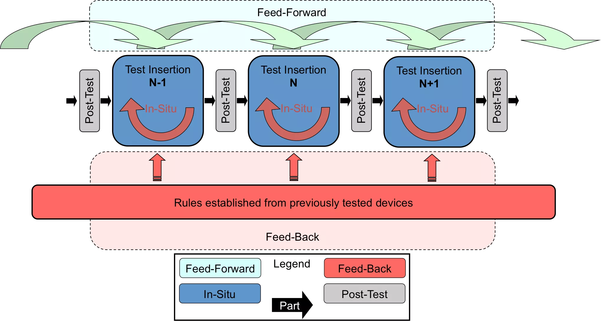
The RITdb group has been working on the next-generation format following STDF to allow more flexibility in data types and support for adaptive test. The group aims to provide a standards-driven data environment for semiconductor test including simple standards-based data capture, transport and relationship model for eTest, probe, and final test data. Its work also seeks to support equipment configuration management and operational performance data. More importantly, RITdb enables a real-time streaming model that provides the ability to collect and monitor data/systems from sand to landfill.

Real Time Adaptive Test (Courtesy HIR)
Work by the RITdb group will ultimately be developed into SEMI Standards. The SEMI Standard spec will be in MS Word while the database itself in a different format. A spec editor will help ensure it is used correctly. The group also plans to expand the spec beyond probe and final test. Meanwhile, the group is working to streamline RITdb and implement different extensions (e.g., tester log, streaming). Additional work will be needed on probe maps and test cases (i.e., be able to run verifiers to validate the spec).
Tester Event Messaging for Semiconductors (TEMS)
Today, semiconductor testing continues to see a surging demand for real-time data analysis, real-time ATE input and control of the test flow to improve test yield, throughput, efficiency, and product quality. At the same time, test equipment and test operations around the world use a diverse range of data formats, specifications, and interface requirements that drive up customer service and application engineering costs for ATE vendors, OSAT companies, IDM test operations, software providers, and handler equipment. A common ATE hardware and software communications interface would help reduce the cost, time and complexity of integrating ATE equipment into data-intensive test operations.

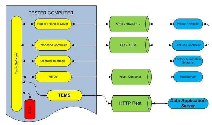
Overview of Test Cell Communication
The TEMS group was chartered to develop a standardized ATE data messaging system based on industry-standard internet communication protocols between a test cell host and a server. The standard will be limited to ATE data messaging, using RITdb entity types as applicable, standard data format, and control requirements. It will have no impact on other test communication interfaces such as those involving handlers, probers, test instrumentation, and other systems covered by existing standards (e.g., SEMI E30, E4, E5, STDF).
The group is developing a set of standards to define a vendor-neutral way to collect test cell data. The primary spec defines the model while a subordinate spec defines the transport layer to maintain consistency with prior standards.
Chip ID & Traceability
Chip ID & Traceability is the most recent group formed under CAST. The group’s formation came on the heels of the 2017 CAST Workshop that focused on Component System Level Test. SLT is widely considered a burden that most chip manufacturers prefer to avoid, but it is essential to achieving lower DPPM (Defective Parts Per Million) goals at system level. The cost to develop and maintain SLT equipment in-house and at OSATS is significant. SLT test engineering requires different skills than regular ATE test engineering. The engineers must understand the final application environment and the data flow that is subjected to the component. Defect causes need to be isolated and communicated back to the vendor or ATE test engineer for corrective action. Mapping such SLT failures back to the ATE production tests is a big, labor-intensive challenge.
Component traceability is a big concern. Most newer technologies have ECID (Electronic Chip Identification). However, many product types representing significant volumes do not provide ID traceability. Without component-level traceability, it is extremely difficult to analyze failures and drive corrective action. Additionally, there is basic manufacturing data, including chip ID, that is needed across the supply chain, but this is often blocked and difficult to obtain from suppliers. Such data analysis is difficult across "silos" due to sharing/security barriers.

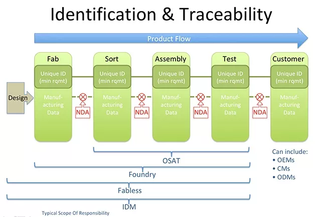
Die-level Identification & Traceability (I&T) Model
The Chip ID & Traceability group was chartered to develop a standardized approach for enabling traceable die-level identification (ID) throughout the IC manufacturing, test, and assembly processes to the point of use in the final system. The approach defines the use of a simple, unique identifier that IC suppliers and board-level manufacturers can use to communicate about a specific device for the purposes of performance or failure analysis. The identifier will enable suppliers and customers to communicate specific component information and, with NDAs (non-disclosure agreements) in place, send manufacturing data back and forward through the supply chain for data analysis.
The group is developing a standardized model focusing on key concepts, behaviors, and requirements for enabling die ID and traceability. The model defines minimum chip ID and traceability for new design and manufacturing implementation as well as for backwards compatibility with existing methods. The resulting standard would apply to different chip configurations ranging from single integrated circuits to multi-chip/3D structures. It can be adapted for use with a range of technologies, ranging from legacy systems to the latest in electronic chip identification (ECID). A copy of the draft proposal can be downloaded here. The Chip ID & Traceability group is soliciting feedback to the document. Please contact Paul Trio at SEMI (ptrio@semi.org).