Risk management, innovation, diversity, and collaboration are key drivers of sustainable semiconductor industry growth and fab management optimization.
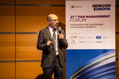
The chip industry is facing a tremendous manufacturing capacity challenge: the industry is expected to reach $1 trillion in annual global revenue by around 2030, up from an estimated $600 billion in 2023. It also under pressure from society, governments, and the industry’s own workforce to operate more sustainably. Balancing the industry’s work to reach net zero emissions while maintaining robust growth presents a formidable challenge. With fab operation optimization a critical part of the solution, the 27th Fab Management Forum gathered industry experts to explore best practices for semiconductor manufacturers to follow.
Intelligent risk-taking on a grand scale
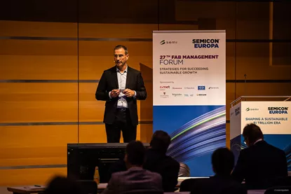
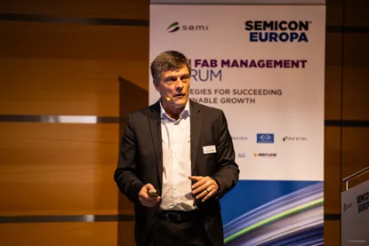
The industry’s growth requires a dramatic expansion in manufacturing capacity over a short timeframe, requiring semiconductor companies to make large bets on the future. The European Chips Act, and strong support from national, regional and local governments, are helping many companies to mitigate the risks to the resilience of the European manufacturing supply chain. One example is Wolfspeed, which is building the world’s largest 200mm silicon carbide (SiC) fab in Saarland, Germany. Keynote speaker Missy Stigall, Senior VP for Global Fab Operations at Wolfspeed, noted: “The availability of financial incentives to build in Saarland influenced our choice of location, but the availability of a local workforce was equally important – Saarland needs the jobs.”
Successful deployment of the new capacity will depend on innovation. According to Stigall, Wolfspeed will need to develop a considerable number of new tools in-house because today’s tools, designed for 300mm silicon wafers, are not ideal for 200mm SiCs.
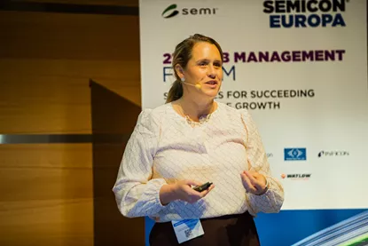
Missy Stigall, Senior VP for Global Fab Operations, Wolfspeed
In Germany, Infineon is investing €5 billion to build its new Smart Power fab alongside existing 200mm and 300mm fabs in Dresden. The new fab, covering an area of 30.000m2, includes 20.000m2 of cleanroom space spread over two floors, and will create 1,000 new jobs.
The ecosystem of semiconductor industry suppliers is also bringing innovation to bear on the manufacturing capacity challenge. Peter Lendermann, Chief Business Development Officer of D-SIMLAB Technologies, described how specialized software can optimize the capacity load mix, enabling fabs maximize production without over-committing to their fab capacity capabilities.
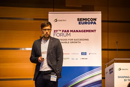
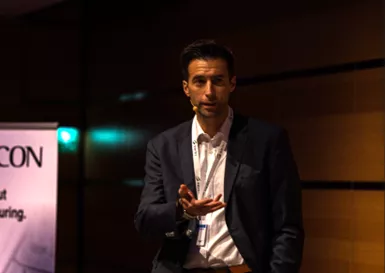
Jamie Potter, CEO of Flexciton, also offered a software solution to fab capacity challenges. He noted, “The problems we are facing are due to the complexity of three semiconductor manufacturing aspects: products, supply chain, and a shortage of skilled workforce able to solve these complex problems. It’s the ideal situation in which to deploy artificial intelligence-based software.”
Jamie Potter, CEO, Flexciton
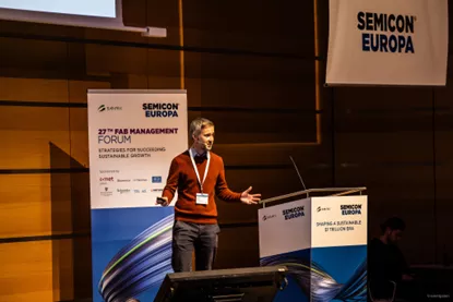
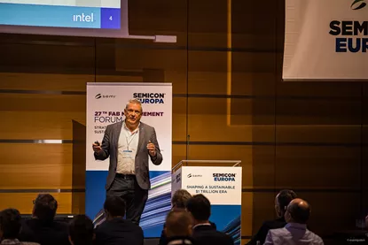
Michael Woittennek, CEO of X-FAB, said the company has built a semiconductor fabrication plant in Dresden. The plant has added new gallium nitride (GaN) capacity alongside existing silicon processes. Woittennek explained the challenge of “the conflict between today and tomorrow” and presented his formula for a successful expansion of an existing facility: “Begin with the end result in mind, measure what matters, and visualize progress and setbacks for the whole fab community – this is crucial for motivating your team.”
Michael Woittennek, CEO, X-FAB
People at the heart of growth: taking stock of the industry’s talent pipeline
X-FAB’s perspective highlighted the vital importance of expanding the talent pipeline to the industry’s growth because of the global shortage of skilled workers at all levels.
Cassandra Melvin, Senior Director of Business Development and Operations at SEMI Europe, identified the industry’s image as a key factor affecting talent acquisition, noting a McKinsey & Company survey that found that the semiconductor industry ranked lower than the tech and automotive sectors on many important criteria including culture and values, diversity and inclusion, work-life-balance, senior management, compensation and benefits, and career opportunities. The success of the European Chips Act relies not only on securing funding and building infrastructure, but also on addressing a critical talent crisis within the semiconductor industry.
“The under-utilized pipeline for essential jobs poses a significant challenge to meeting the Act’s ambitious goals,” Melvin said. “Acknowledging the industry’s existing image challenges is crucial, as overcoming them is vital for attracting the skilled workforce required for imminent industry growth. If we don’t prioritize workplace culture and inclusion – and value people – success in achieving the objectives of the European Chips Act remains at risk.”
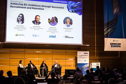
Left to right: Cassandra Melvin, Senior Director of Business Development and Operations, SEMI Europe; Richard Goddard, Global Practice Lead, Technology, Mercuriurval; Michelle Williams-Vaden, Deputy Director of the SEMI Foundation; Bernard Capraro, EU Talent Programme Manager, Intel.
Intel faces this problem acutely, because of its plans to expand European production capacity in Ireland, Germany and Poland. Bernard Capraro, EU Talent Program Manager at Intel, highlighted the company’s unfilled demand for technician. “Approximately 70% of the technical staff employed in a fab belongs to the technician level – they are the most important people on site. Without these people, you are nothing – the problem of recruiting them is what keeps me awake at night,” Capraro said.
A panel discussion highlighted the instrumental role of universities and governments in supporting the industry’s growth and focused on what organizations can do now to start building the talent pipeline of the future, one of which included raising its profiles in schools and colleges. “Teachers are particularly strong influencers,” Capraro said.
Bernard Capraro, EU Talent Program Manager, Intel
Michelle Williams-Vaden, Deputy Director of the SEMI Foundation, noted that the industry should treat diversity, equity, inclusion and belonging (DEIB) initiatives as part of the solution, because they expand the talent pool. “DEIB is not a soft thing, it should be a central business strategy,” she advised. “Research shows that diverse teams produce more creativity and productivity. Add one outsider to a fixed team, and you will double your chance of finding a solution to a problem that the team has been struggling with.”
The ambition of sustainable growth and prosperity
Fabien Chene, VP of Sustainability Solutions at Schneider Electric, addressed another challenge facing the semiconductor industry in its ambition to achieve sustainable growth The company’s framework for sustainable growth is based on three strands, he explained: “Strategize, to create a decarbonization roadmap. Digitize, to monitor progress. And decarbonize, through electrification and power savings.”
Fabien Chene, VP of Sustainability Solutions, Schneider Electric
With increases in operational efficiency improving energy efficiency, Dionys van de Ven, President of the Industrial IXS Division at Comet Yxlon, presented a new way to advance the yield of advanced packaging products: “Killer defects in advanced packaging ICs are not systematic, and we cannot run destructive testing to find them,” he said. van de Ven described a new X-ray inspection tool, the CA20, which generates 3D volumetric images rather than 2D slices of features such as microbumps. “With this new tool, engineers can inspect faster in the ramp-up and production phases, and speed up failure analysis,” he added.
Dionys van de Ven, President of the Industrial X-Ray Systems (IXS) Division, Comet Yxlon
Increasing efficiency even further is the goal of the autonomous fab, a concept described by John Behnke, General Manager of Inficon. “Inspection analysis based on engineers’ intuition and experience is getting harder because of the increased fab manufacturing complexity and the shortage of experienced talent,” Behnke said. “We need to move to a fab management model based on AI-enabled software alongside digital twin simulation and traditional scheduling tools.”
John Behnke, General Manager, Inficon
The themes of operational efficiency and sustainability ran through the day’s discussions. As session chair Simone Alba of STMicroelectronics observed, “Improving fab efficiency is a common goal for us all, because it is good for profitability, but also good for sustainable growth and the path to net zero.”
Simone Alba, Dry Etch Area Manager, STMicroelectronics
The Fab Management Forum will return to SEMICON Europa, co-located with electronica, on November 13, 2024.
On behalf of SEMI, the SEMI Europe team thanks the Fab Management Forum committee members for their tremendous work in creating a top-notch program as well as industry leaders for sharing their views during the 27th Fab Management Forum.
Serena Brischetto is Director of Marketing and Digital Engagement at SEMI Europe.