downloadGroupGroupnoun_press release_995423_000000 copyGroupnoun_Feed_96767_000000Group 19noun_pictures_1817522_000000Member company iconResource item iconStore item iconGroup 19Group 19noun_Photo_2085192_000000 Copynoun_presentation_2096081_000000Group 19Group Copy 7noun_webinar_692730_000000Path
Skip to main content

Meeting Metrology and Inspection Requirements as EUVL Ramps Up for 5nm and 3nm

The Advanced Lithography TechXPOT at this year’s SEMICON West will explore progress in extreme ultraviolet lithography (EUVL), its economic viability for high-volume manufacturing (HVM) and other lithography solutions that will address the march to 5nm and onward to 3nm.As a prelude to the event,...

SEMICON West Preview: Materials and Subsystem Suppliers Find Solutions to Emerging Wafer Defectivity Issues at Small Geometries

New metrology and inspection technologies and new analysis approaches made possible by improving compute technology offer solutions to finding the increasingly subtle variations in materials and subsystems that meet specifications but still cause defects on the wafer. More collaboration across the...

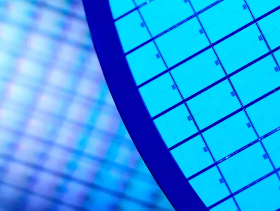
Metrology and Inspection Challenges at 5nm and Beyond

The Scaling Technologies TechXPOT at this year’s SEMICON West (Scaling Every Which Way! – Thursday, July 12, 2:00pm-4:00pm) will explore traditional scaling as the industry marches toward 3nm and beyond, as well as technologies that enable 3D architectures, die stacking, and interconnect scaling....