
Advanced Packaging Hailed as Engine of Moore’s Law Scaling
It has taken decades of research and development and strong commitment to various industry programs, but the stars are finally aligning for 3D semiconductor systems. No one could have left the 3D & Systems Summit 2023 – held in late June in Dresden – with any doubt that heterogeneous integration, enabled by increasingly mature 3D packaging technologies, is becoming a key driver of the semiconductor industry’s success.
The rise of heterogeneous integration is being fueled by new patterns of demand for electronics systems. As Laith Altimime, President of SEMI Europe, explained in his opening remarks at the summit, “Rather than just one megatrend as in the past, we have several megatrends at the same time – autonomous vehicles, 5G and soon 6G connectivity, the IoT, and artificial intelligence – driving the exponential growth to $1 trillion industry by 2030.”
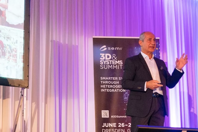
Laith Altimime, President of SEMI Europe
At the same time, traditional transistor scaling is facing challenges. Seung Kang, Vice President of Strategy at Adeia, pointed to one example: “SRAM scaling stalled at 5nm, and this is bad news: in a typical SoC, 30% of the die area is taken up by SRAM.”
New megatrend applications do not benefit from transistor scaling in the way the PC does, thus the industry is turning to heterogeneous integration as the way to improve performance, power, area and cost (PPAC). Rozalia Beica, VP of Strategic Marketing and Business Development at AT&S, painted a vision of new types of AI-enabled processor chips that rely on “a heterogeneous set of chiplets built on various nodes and processes that are optimized for each different function.”
Seung Kang, VP of Strategy at Adeia
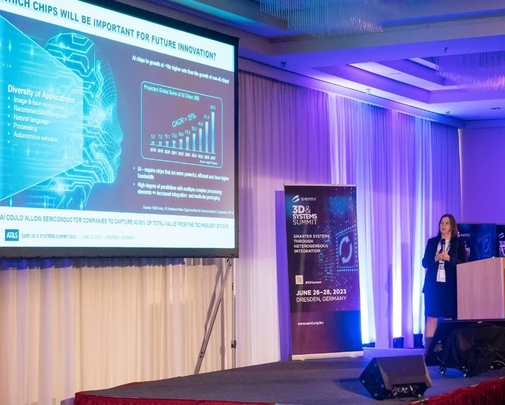
Rozalia Beica, VP of Strategic Marketing and Business Development at AT&S
The potential for heterogeneous integration to produce real-world results was expressed by Raja Swaminathan, Corporate Vice President at AMD. He said, “In applications such as AI and high-performance computing, scaling of the vertical interconnect is producing stunning improvements in efficiency and density. In my view, hybrid bonding is now the technology to drive Moore’s Law improvements in PPAC.”
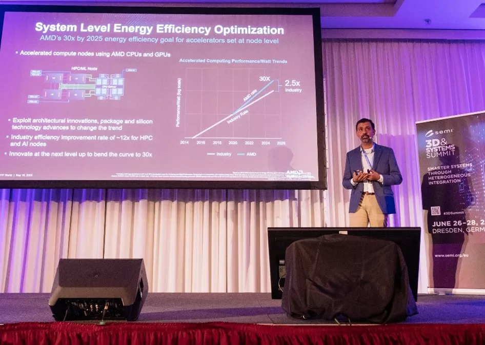
Raja Swaminathan, Corporate VO at AMD
No Single Way to Achieve Heterogeneous Integration
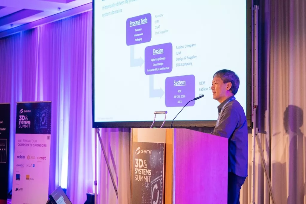
Beyond the world of high-performance computing, others at the summit showed how advanced packaging can be implemented broadly in SoCs and ASICs. Emilie Jolivet, Director of the Semiconductor, Memory, and Computing Division at YOLE Group, highlighted that chiplet architectures enable large chips to use lower-cost mature nodes for parts of their functionality, such as analog, RF, and non-volatile memory.
Evidence of the appeal of new packaging techniques for integrating heterogeneous functions came from André Blum, Project Manager of the Progressive Semiconductor Program at the Volkswagen Group. He cited an example in which Audi “was able to achieve a 90% reduction in the volume of an exterior door handle assembly through the stacking of active and passive components.” He also noted the value in Audi’s collaboration with the SEMI Global Automotive Advisory Council, which connects the automotive and semiconductor ecosystems, and invited stakeholders across the two industries to collaborate with Audi.
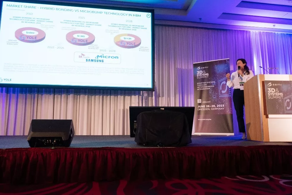
Emilie Jolivet, Director of the Semiconductor, Memory, and Computing Division at YOLE Group
André Blum, Project Manager of the Progressive Semiconductor Program at the Volkswagen Group
Democratizing Heterogeneous Integration Technologies
The advanced packaging techniques used today in 2.5D and 3D stacked chips are costly to implement and call for considerable technical resources. One driver of the expanding adoption of chiplet-based architectures is MOSAICS-LP, a scalable platform for integrating chiplets in edge computing applications, said Yoan Dupret, Managing Director and Chief Technology Officer of Menta. Dupret said the platform “provides a way to re-use chiplets across devices, to make chiplets easy to design, and to reduce the barriers to entry into the heterogeneous integration market.”
New Advances in Packaging Technology Support Heterogeneous Integration
The adoption of 2.5D and 3D packaging by AMD, Audi and other influential companies demonstrate that the technologies are being deployed in volume today, yet challenges to their widespread use remain. Jan Vardaman, President and Founder of TechSearch International, stressed the need for design tools that can accelerate 3D systems development, noting that “We need EDA tools and the people who know how to use them. We also need better interfaces between EDA tools.”
Jan Vardaman, President and Founder of TechSearch International
What EDA lets designers create the fab must be able to build. That’s why much of the summit focused on manufacturing vertically integrated chips.
Pascal Metzger, Chief Executive Officer of SET Corporation, explained the extraordinary levels of precision and tolerances required in the hybrid bonding process – even vibrations coming through the fab floor from the surrounding environment can disturb bonding equipment. Metzger noted, “When you are shooting for accuracy of ±1µm in hybrid bonding, every factor counts, and you have to manage them all carefully.”
Pascal Metzger, CEO of SET Corporation
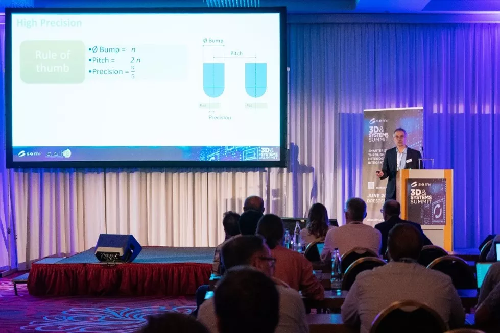
Several speakers were keen to tell the summit that direct bonding is not the only approach to building 2.5D and 3D systems: imec’s roadmap for microbumps shows a path to pitch spacing down to just 5µm. Anne Jourdain, Principal Member of Technical Staff and Team Lead for 3D Heterogeneous Integration at imec outlined the advanced chemistry research that is enabling microbumps to maintain bond strength and mechanical integrity as the size of the ball shrinks. She said, “A solder-based technology is a valid option for chiplet-based die-to-wafer and memory applications and can be much more easily used in current process flows than direct bonding can.”
The integrity of hybrid bonding and microbump interconnects can only be validated by reliable test methods, which is more challenging with fine pitch and 3D structures. Inspection methods such as e-beam and optical have limitations as well, and therefore the need for new inspection methods is approaching.
Isabella Drolz, Vice President of Product Marketing at Comet Yxlon, emphasized the benefits of employing cutting-edge non-destructive 3D X-ray inspection technology in advanced packaging processes, saying that "X-ray imaging can identify killer defects in complex 3D chip designs in mere minutes what would typically require days.”
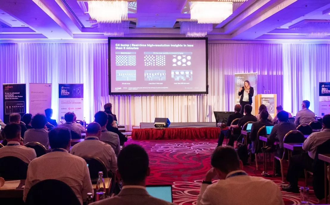
Isabella Drolz, VP of Product Marketing at Comet Yxlon
During his talk, Putting Light into Your Chips: Heterogeneous Integration of InP Photonics, Luc Augustin, Chief Technology Officer of Smart Photonics, described how the smart photonics foundry provides a platform for building integrated photonics components, including a PDK toolbox and more than 50 IP building blocks, that will be familiar to electronics engineers.
Heterogeneous Integration Delivering on its Promise
Eric Beyne, Senior Fellow, Vice President of R&D and Director of 3D System Integration Program of imec, highlighted the vast interest in and bright future for 2.5D and 3D system technologies. “There are lots of challenges, but there are also many solutions in development or already in use,” he said. “Perhaps the biggest challenge now is at system level: chip designers and system architects have to get their heads around what the new heterogeneous integration architectures can enable.” He also cited the need for design technology co-optimization alongside system technology co-optimization. The unused potential of these system architectures is the most exciting prospect of all, presenting countless opportunities for collaboration across the value chain.
Left to Right: Jan Vardaman, President and Founder of TechSearch International; Eric Beyne, Senior Fellow, Vice President of R&D and Director of 3D System Integration Program of imec; André Blum, Project Manager of the Progressive Semiconductor Program at the Volkswagen Group; Raja Swaminathan, Corporate VP at AMD
Altimime closed the summit with a summary of the opportunities and challenges ahead for the semiconductor industry to reach $1 trillion in revenue by 2030 – those technical, economical, and environmental. Referencing Beica’s talk, he reiterated that chiplets and heterogeneous integration will transform the chip industry and enable new architectures and integration approaches to drive higher performance, cost efficiencies and customization while speeding time-to-market and reducing development costs.
He emphasized that only through collaboration across the value chain will the industry be able to overcome challenges and provide timely, cost-effective, and sustainable technology solutions.
Dirk Hilbert, Mayor of City of Dresden (left); Laith Altimime, President of SEMI Europe (right) during SEMI Networking Dinner Cruise on the River Elbe
Cassandra Melvin is senior director of Business Development and Operation at SEMI.