Creating a custom Internet of Things (IoT) IC is challenging because it involves multiple design domains (digital, analog and RF). Creating a sensor-based IC that combines electronics that use the traditional CMOS IC design flow with a MEMS sensor on the same silicon die, however, can seem impossible. Couple the co-design and verification challenges with a lack of traditional process design kit (PDK) support for MEMS, and you have a tough road to travel to get your IoT designs to market.
What can we do to make the sensor-based IoT design community successful?
Understanding the Challenges
The sensor-based IoT IC typically features a MEMS sensor (and optional actuator) that interact with the real world. Analog and digital circuitry processes the signals and sends them to a CPU. The CPU provides the “smarts” to process the data from the sensor and then sends processed data via a radio to the Internet; alternatively, the CPU could activate the actuator.
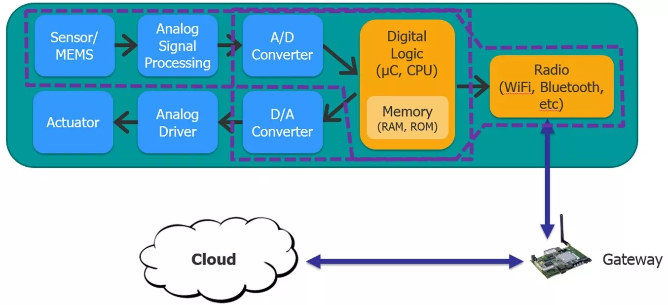
A typical sensor-based IoT IC (Source: Mentor: A Siemens Business)
Based on the complexity of the system, designers face many co-design challenges:
- Analog design requirements imposed by MEMS: MEMS devices often require high voltages and multiple power supplies; they emit small signals that need amplification and conditioning; and they are sensitive to the environment and require calibration.
- Design flow interactions: Parasitics from MEMS devices might affect circuits and vice versa. Circuit designers need MEMS models for impedance and timing.
- Integration: MEMS devices operate at different timescales than circuits, which adds a layer of complexity. Compounding the problem is a lack of MEMS PDKs and methods to tie together ICs and MEMS PDKs for integration and cross-verification.
After conquering the co-design challenges, the design team has to address mixed-domain simulation challenges that include:
- Simulating the system: This requires verification of MEMS, digital, analog and RF circuitry with embedded software that runs on the CPU.
- Timescales: These vary widely, from a single deflection of the MEMS transducer in femtoseconds to a seconds-long simulation of the embedded software performing a measurement and transmitting data.
- Simulation time: Simulation of a behavioral digital design is extremely fast. However, the system simulation requires stand-in models that incorporate the behavior of the analog and MEMS block to simulate in an acceptable amount of time.
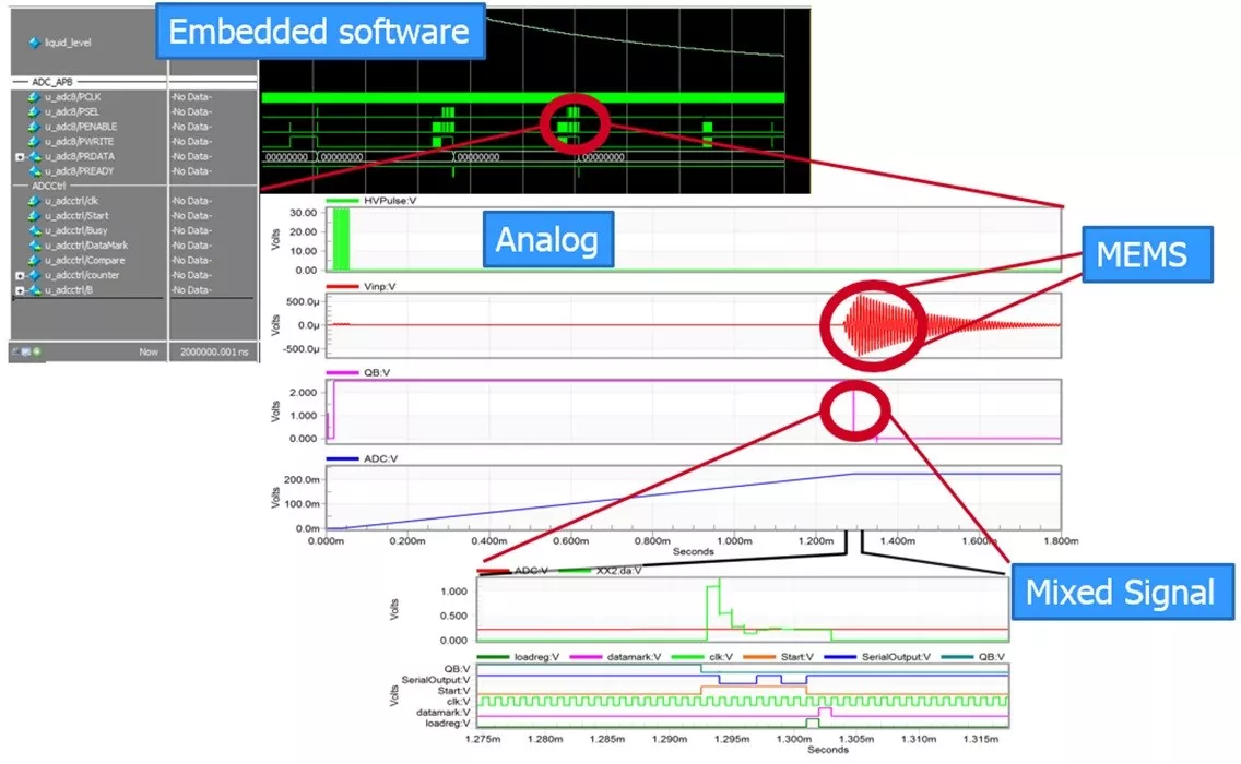
The challenge of timescales for co-simulation. (Source: Mentor: A Siemens Business)
MEMS is the Key
The reality is that it’s the MEMS device that adds extra complexity to the sensor-based IC design and verification flow. To amplify the problem, the MEMS manufacturing process is not nearly as mature as the standardized IC process. For example, the standardized IC process includes ready-made PDKs that include everything designers need to move through design and verification flows. Foundries often provide soft and hard IP to quickly build-out design, and EDA tools provide high levels of automation enabled by abstraction and a standardized IC flow. How will MEMS-based design evolve?
MEMS-based design must catch up to the standardized IC process. The first step is providing MEMS PDKs that include:
- Multi-physics domain design rules and material properties
- Packaging information
- Wafer and bonding information
- Fabrication information
We must also tackle issues associated with these PDKs, including:
- Ownership, distribution and maintenance of the PDKs
- Consensus on the contents of the PDKs
- Merging of CMOS and MEMS PDKs
The industry needs to move toward standardized MEMS manufacturing processes with available PDKs. Companies must provide IP and recommend structured design methods for co-design and verification of ICs that incorporate MEMS. How can EDA help with these flows?
The EDA Contribution
EDA companies must work with teams in the MEMS IC co-design space, collaborating with MEMS fabricators to help enable PDKs. By incorporating PDK support within their own tools, EDA companies can provide an integrated custom IC flow that allows teams to design and verify MEMS-based ICs. For details about this flow, click here to download the Mentor whitepaper: Fusing CMOS IC and MEMS Design for IoT Edge Devices.
 Greg Lebsack brings 25 years of executive and technical management experience — along with a proven track record of building strong teams and delivering predictable results — to his role as general manager of the ICDS division of Mentor, a Siemens Business. Lebsack joined Mentor in 2015 after that company acquired Tanner EDA, where he was president. Prior to Tanner EDA, he held management and technical positions in a number of different industries and companies, including Sprint, General Electric and McKinsey & Co. Greg holds a bachelor’s degree in business administration from Northern Arizona University.
Greg Lebsack recently presented on the topic of Integrated Co-design of MEMS/IC at the MEMS & Sensors Technical congress, a technical conference organized by the MEMS & Sensors Industry Group.