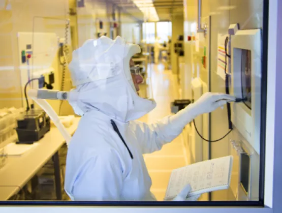
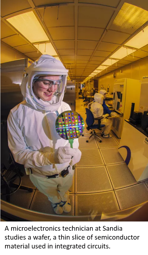
Sandia National Laboratories just finished updating equipment in its microelectronics fab, marking the completion of the first phase of a 3-year fab upgrade program. The transition from 6-inch to 8-inch wafer sizes will align the Department of Energy national lab with industry standards to ensure easier access to tools, spare parts and raw materials.
Sandia is a prestigious member of the SEMI Fab Owners Alliance (SEMI FOA), an international group of semiconductor and MEMS fab managers and industry suppliers that meet regularly to solve common non-competitive manufacturing issues and improve their business results. SEMI spoke with Michael Holmes, senior manager of microfabrication at Sandia, about its approach to revitalizing the fab while developing new production processes and technologies.

SEMI: What were the main challenges in moving into production with 8-inch wafers?
Holmes: The goal of the conversion is to reestablish our 6-inch production processes on 8-inch wafers including our radiation hardened 350nm CMOS and MEMS technologies. This requires tuning hundreds of interrelated parameters to get the same end result as before but with different equipment and at a larger scale. In addition, during the conversion we are developing a new 180nm radiation hardened CMOS production process and re-establishing research work on 8” in our silicon photonics and ion trap technologies. Modifications to the facility have also been required including raising the ceiling to install the new implanter and relocating our gowning area to facilitate installation of new CMP tools. In addition to converting our Silicon fabrication facility, we are also converting select equipment in our compound semiconductor facility. We are one large team working toward these goals.
SEMI: Were there any roadblocks in sustaining production of the 6-inch wafers while planning and implementing processes for the upgrade to 8-inch?
Holmes: Six years of planning ensured the conversion would not affect production of components needed for national defense. This planning window was required to ensure production commitments were completed in advance of conversion start in August of 2018 and return to production for commitments starting in July 2021. This period provides time to complete the hardware conversion and steps review and requalify the production line to ensure products made using the new equipment are identical to ones produced by the old equipment. The hardware conversion phase completed on schedule and the fabrication of prototype and research components on 8-inch started in November of 2018.
 SEMI: Can you shed some light on the development of gold antennas that promise to improve the thermal infrared radiation capabilities in systems?
Holmes: Sandia developed a new infrared detector design that breaks away from relying on thick layers of detector material and instead uses a subwavelength nanoantenna – a patterned array of gold square or cross shapes – to concentrate light on a thinner layer of material. This design uses just a fraction of a micron of detector material, whereas traditional thermal infrared detectors have a thickness of 5 to 10 microns. The nanoantenna-enhanced design increases the amount of an infrared radiation a detector can see while also reducing image distortion caused by background noise. It also allows for the invention of new detector concepts.
SEMI: Sandia is known for producing high-reliability components. Several SEMI FOA members have customers in the automotive domain, where reliability is critical. Do you have any advice for them on their path to high-reliability, zero-defect systems?
Holmes: High-reliability microdevices at Sandia’s MESA facility are paramount. A structured quality program is rigorously realized in each facet of the production process. Our processes and design rules are constructed around reliability, and we extensively leverage in-line metrology and electrical test to validate devices throughout production.
SEMI: Are there any examples of how the FOA peer-to-peer dialogue and knowledge sharing helped in your upgrade from 6-inch to 8-inch?
Holmes: Sandia is new to the FOA. Our initial interactions have been very valuable, and members have shared insights into metrics and process improvements that will benefit MESA moving forward. Relative to the 6-inch to 8-inch conversion, as part of our planning process, we did engage other foundries within the FOA to solicit feedback and lessons learned.

The mission of the Fab Owners Alliance is to provide value to the fab management and operations community through collaborative platforms for device makers and solution providers.
Nishita Rao is marketing manager for technology communities at SEMI.