Belgium-based Sigasi, a member of the ESD Alliance, a SEMI Technology Community, is a digital chip design validation company that firmly believes in the shift-left methodology to get chip designs right the first time. Sigasi has developed an Integrated Design Environment (IDE) that does just that. Shift-left means implementing quality control, design checks, and verification as early as possible in the project cycle to catch––and correct––problems promptly.
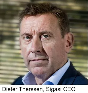
I spoke with Sigasi CEO Dieter Therssen about the challenges in the design and verification markets and what Sigasi is observing.
Smith: What trends are you seeing? Do any surprise you?
Therssen: There are absolutely two major trends that nobody should ignore: the tenacity of Moore’s Law and the pervasiveness of Artificial Intelligence (AI).
Moore’s Law, which sets the bar for growth in the semiconductor industry, has always been working against a ceiling of physical limitations. Indeed, there are theories waiting in the wings to replace it, like Neven’s Law, which is concerned with quantum computing. But the takeover has not yet happened, and Moore’s Law is still alive and kicking, relevant as ever. Our manufacturing friends in the semiconductor world certainly have been very creative in extending lithography to the cutting edge with Extreme Ultraviolet (EUV) light, reinventing the transistor with the Gate All Around (GAA) architecture, and experimenting with super atomic materials.
Even at 2nm, we’re still going strong, fitting hundreds of billions of transistors on a single device.
What’s surprising is how impressively the Electronic Design Automation (EDA) market—the shy sibling in the semiconductor market family—has been adapting to the capacity predicted by Moore’s Law for almost 60 years now! Most people forget that not only are miracles happening in the manufacturing world, but IC design tools need to keep up with the gigantic capacities. That said, the EDA workflow needs to adapt once again: a simple register transfer level (RTL) editor, followed by simulation/emulation for validation will no longer do.
 If designers cannot test for errors as soon as possible during front-end design, there’s a real risk of incurring the huge cost of new mask sets. I wouldn't want to be the designer who overlooks a clock edge issue somewhere in the design and then needs to order $30 million worth of new masks. Writing RTL has changed a lot from when I started doing silicon design; it now calls for adopting the shift-left mentality as much as possible. IDEs are a must. RTL must be developed and validated simultaneously, beyond simple syntax checking. Designs need real-time introspecting and integrated library components so that they can be handed off to simulation and implementation teams with confidence the first time around.
The second trend is pervasive AI. Words fail to capture how fast and far reaching this technology is affecting everything. Every chip under development now needs hardware to support the computations that underlay AI—tensor processing, inference engines, transformers, and the like. Moreover, every utility, tool, and application we have developed in the past is being challenged to transform itself to accommodate and deploy AI. We’re not being asked to optimize existing recipes created for the task at hand, but to fundamentally rethink how the original problem can be addressed in a revolutionary way.
Semiconductor companies cannot afford to watch from the sidelines as AI reshapes how things are done in their industry. Operations at almost every aspect of design, manufacturing, and packaging need to consider how AI can improve their part of the business.
Smith: What are some of the challenges for developers writing code, be it SystemVerilog or VHDL? What poses the biggest risk? Is it the design, the schedule, or the integrity of the device?
Therssen: The biggest challenge for an RTL designer is complexity, the need to be able to manage all the risks. Even an expert RTL coder can’t keep track of all the requirements for the appropriate coding style. Safety measures, security vulnerabilities, Power/Performance/Area (PPA) constraints all impose rules and measures that need to be addressed in RTL, before the specification can be handed off.
The integrity of the RTL design is the end goal here. The specification needs to correspond to the intent. This means that the RTL test bench is probably even more important than the RTL design: it is the test bench that makes sure that the design does what it is supposed to do, even under unexpected circumstances. Verification methodologies such as UVM facilitate writing good test benches, but that adds yet another set of requirements to the already extensive list that the poor RTL designer needs to check.
Your question speaks to comparing hardware description languages SystemVerilog and VHDL in this context of coding challenges. But even that is no longer an exclusive scenario: integrating RTL leads to mixing the languages, where the ideal library or IP might not be available in the preferred RTL language. Actually, this integration puts yet another set of requirements in place, where you want to make sure that the RTL modules and entities are interfacing as intended, and so on.
The nature of IC-bound applications and test benches makes for hundreds of files each containing thousands of lines of code where you need to be vigilant—and some RTL designers need to be vigilant in a language that might not be their strong suit. Doing so up to standard is no longer possible in a traditional specification environment.
If these challenges are not tracked efficiently, the result is clear: the schedule slips. The schedule itself is usually not the root problem. The schedule is reasonable enough, if the real challenges are managed with a certain amount of automation, inside an integrated design environment.
Smith: When engineers talk about designing a chip, an SoC or a system, most will say verification is 70% of the overall time because of complexity and the enormous cost of making a mistake.
Therssen: Let’s start by agreeing that verification is extremely important and claims a substantial portion of an IC design project’s schedule.
We hear from some customers that verification consumes 70% of the design cycle prior to physical implementation. Others tell us it is more one to one, so it is a little hard to generalize. This could be due to how companies think about their organizations and managerial separations.
 It all comes down to definitions: what is verification and who’s doing it? Companies that have clearly defined groups that manage design or verification would track resource hours by group and then make the calculation. Yet even in that situation, there will be confusion because formal verification is sometimes executed by the creation team, whereas the verification team prefers to focus on dynamic verification. This situation is aggravated because the verification number usually doesn’t have a well-defined unit. Are we talking about the engineering effort to start a simulation and analyze the results, or the lengthy wall clock time spent by computers in simulation and emulation runs?
On the other hand, the argument for shift-left is that design and verification become one activity that needs to be team-managed. In that case, it is difficult to calculate a meaningful percentage.
For Sigasi, the number is irrelevant: we monitor design creation and design verification engineers with the same engine, with real-time feedback about the integrity of the RTL design under test and the RTL verification framework. The ability to hand this RTL off with confidence leads to fewer iterations between the RTL specification and RTL verification portions of the workflow—and that makes the difference between a project being on schedule or not. Where this productivity gain is counted is just a formality to us.
Smith: What about FPGA designs? Is the front-end design the same or is it fundamentally different?
Therssen: The swing towards better managing complexity in front-end design is exactly the same. The rules that need to be enforced are different.
An FPGA imposes extra requirements so that an application can be mapped on some specialized pre-defined architectures (DSP elements, memory components, clock and reset trees). So, the need for a development environment that enforces the correct coding style is even more important here.
Ultimately, the front-end design flow remains shared between ASIC and FPGA designers. However, the impact of mistakes isn’t the same. I’ve already mentioned that a mistake for an ASIC design often leads to a costly respin (tens of millions of dollars in new masks, for example). A mistake for an FPGA design is discovered faster and fixed at minimal cost (a few days of engineering).
Smith: Our industry talks about the open-source movement that spans EDA design and verification tools and IP. What are you seeing and how would that or could that affect front-end design?
Therssen: Let’s start with the IP portion of this question. The world runs on semiconductor hardware. But all that hardware is ultimately controlled by software. An example would be NVidia. I personally would consider them a hardware company, but now, probably motivated by AI, they’re positioning themselves as a software company providing full-stack solutions that run on their hardware. Why does it matter? My point is that the open-source community is mainly driven to where the action is, and software is where the action is.
Going back to your broader question, what about open-source solutions for EDA design and verification tools? Compared to software tools in general, where copious amounts of engineers active in all kinds of applications create plenty of leverage for open-source solutions, the EDA world has inspired relatively little open-source activity. Still some open-source tools do interesting things, but I don’t see a lot of initiatives catching up to the commercial offerings that are already widely used anytime soon.
Case in point: some open-source initiatives claim to do similar things to the products we offer. They look and feel similar, but the width and depth of their ability to help designers is much more limited.
Smith: In other words, you get what you pay for, meaning that a hobbyist or an experimenter might be fine trying out an open-source tool. A designer on deadline to get a new project potentially worth millions of dollars out the door will look at the risk and forgo open-source tools.
Therssen: Exactly! However, an example of where open source does work is the RISC-V movement. It is a special case and probably a good thing in terms of moving our industry forward and away from a single source solution. I believe open RISC-V makes sense for the industry.
Smith: Which markets do you see driving the demand for new chip designs?
Therssen: I think we can refer to the second trend I identified in our first answer: any market that efficiently deploys AI. Those are the markets where the inherent complexity of AI directly translates to complexity of the front-end design flow.
We see this, for example, in the automotive sector, where Advanced Driver-Assistance Systems (ADAS) combined with sophisticated infotainment and hybrid engines has led to an explosion of Electronic Control Units (ECU) needed for cars. Not so long ago, you could find one, maybe two ECUs in a car. Today, you shouldn’t be surprised if you find over 100 ECUs in your hybrid SUV!
We’re also already seeing the advantages of AI in the medical world, resulting in better ways to perform and analyze MRIs, CTs, X-rays, ECGs, and other tests. It seems like every medical acronym opens the door for brand new, AI-deploying chip designs.
Finally, I should mention the Race for Space, which is absolutely on. The competition for exploration, homeland security, communication, and such is leading to opportunities worldwide to create satellites filled with AI-powered ICs. Regardless of quantity in terms of number of chips, in terms of design complexity, it’s challenging. Whether a company makes one or a million chips a year for space applications, they still need to be designed—free of errors.
About Dieter Therssen
Dieter Therssen obtained his master's degree in Electronics Engineering from KU Leuven in 1987 and started his career as a hardware design engineer in the early days of silicon integration using tools from IMEC. Since then, he has worked with leading companies including Philips Semiconductor, NXP, Lear and several others.
As CEO of Sigasi, Dieter leverages his strong semiconductor background and forever enjoys the magic of a motivated group, such as the team he leads at Sigasi.
Robert (Bob) Smith is Executive Director of the ESD Alliance, a SEMI Technology Community.