This article is the third in a series highlighting the vital importance of SEMI Standards to commemorate the publication of the 1000th SEMI Standard in July 2019. Find the entire series here.
SEMI Standards are the bedrock of the modern microelectronics industry. Without standards for wafer dimensions – which SEMI Standards first defined through a collaborative process involving semiconductor manufacturers and wafer suppliers in 1972 – the semiconductor equipment industry as we know it would not exist today.
The late Robert Noyce of Intel noted in this 1992 video “being good at producing semiconductors will mean we have better, more consistent, better controlled equipment than we have in the past. Standards are going to play a vital role in that. Standards saves money and time for everyone.”
 Noyce also called standards a bellwether to surges of innovation in critical process technology. This is still true today as, for example, important standards-setting activity is afoot in panel-level packaging, electron microscopy and energetic materials. Will a surge of innovation follow?
Panel-level packaging: a chicken-egg scenario
From advanced materials to more efficient production tools, one hallmark of the microelectronics industry is our fearless exploration of new technologies that will spawn change across the industry by improving performance and reducing cost. Advanced packaging techniques, such as panel-level packaging (PLP) – which moves semiconductor packaging to a larger-panel format – is one of those critical catalysts. Citing PLP’s potential to shrink costs by improving efficiency and economies of scale, research firm Yole Développement predicts a remarkable 63% CAGR for PLP from 2017-2023.[i]
It’s no stretch to say that we are close to realizing a burst of innovation in packaging. With a just-published SEMI Standard (SEMI 3D20) specifying panel sizes, equipment companies will find it economically viable to invest more in developing the much-needed production tools that enable PLP.
“It is really important to create standards so we come together and work much more efficiently. Creating those fundamentals allows you to be more productive in the long term,” said Christina Chu, ASM Semiconductors, and co-leader of the Panel Level Packaging Task Force, and one of five industry leaders recognized for their outstanding accomplishments in developing SEMI Standards for the electronics and related industries at the recent 1000 SEMI Standards reception during SEMICON West 2019.
“This effort came up from the trenches,” said Richard Allen, NIST Quantum Measurement Division, and a co-leader of both SEMI’s 3D Packaging and Integration Committee and its Panel Level Packaging Task Force. “Equipment vendors told us that they wanted to serve the market, but they couldn’t do so without some standards. To respond to their request, our committee surveyed the market and discovered at least 15 different panel sizes in development.”
“As no vendor is going to make over a dozen unique tools for the same process, we worked with the manufacturers and tool companies to write a specification that standardizes on two of the most widely accepted sizes,” Allen said. “For the first time, the industry will have a real market for panel-level packaging tools, and that will spur commercialization of new technologies that never would have seen the light of the day without standardization.”
Allen pointed out that evolution of standards in microelectronics reflects the dynamism of the microelectronics industry itself. “Given the rate of technology advancement in microelectronics, SEMI Standards committee and task force members know that a newly-published standard is often just a starting point, and change will likely follow,” he said. “The Panel Level Packaging Task Force, for example, is currently determining how to best support this packaging technology, whether through possible enhancements to 3D20 or by creating new PLP standards.”
Process automation is key for TEM
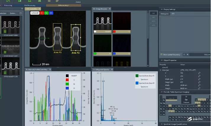
Transmission electron microscopy (TEM) is another area where industry cooperation will fuel progress.
“People throw around the phrase ‘exponential growth,’” said James Amano, senior director, International Standards at SEMI. “It’s usually a gross exaggeration, but not when it comes to TEM data. That’s because demand for more TEM data, which uniquely enables innovations around smaller feature sizes, has exploded. At the same time, TEM data is a bottleneck in the fab. Operators literally use tweezers to carry around electron microscope samples by hand, and that is untenable.”

TEM sampling standards are currently being formulated under the SEMI Standards development process.
“Applying a model that we have employed successfully time and time again through SEMI Standards, we are gearing up for process automation in TEM,” Amano said. “We’ll start by establishing a grid carrier standard for electron microscopy. Through ongoing standards efforts, we may realize a fully automated TEM process within just a few years. That achievement will enable exponential growth in shrinking design geometries.”
Energetic materials gain safety standard
Along with wafer-level packaging and design shrinks, the push for safety in materials’ usage is a hotbed of innovation. This is especially true with energetic materials, the potentially hazardous process chemicals used increasingly in semiconductor manufacturing to spur advances in materials purity, integrity and quality.
“When you’re working with energetic materials, if you don’t get it right, you may face serious yield and cost issues, and most important of all, safety risks,” said Paul Trio, senior manager of strategic initiatives at SEMI. “This isn’t a theoretical concern. Real problems occurring in fabs have made an energetic-materials standard a high priority for the industry.”
“After years of collaborating with companies across the supply chain to address this significant challenge, we recently published our 1000th SEMI Standard around safe usage of energetic materials,” Trio said. “Now manufacturers can turn to a new standard – which will evolve dynamically in response to industry changes – as they employ energetic materials in their quest to achieve higher yields while controlling costs and managing safety risks.”
Whether it’s packaging, design shrinks, materials or other key innovations, standards are essential to progress in microelectronics. From equipment and materials suppliers that provide the most advanced, efficient and safest tools, materials, and processes to device manufacturers that get products to market, all stakeholders in the microelectronics ecosystem benefit from SEMI Standards.
Are you curious about the areas of process technology where innovations are likely to occur? Would you like to get involved in standards efforts that could have an impact on your business? Take a look at the activity of SEMI Standards Committees and Task Forces. Because that’s where innovation, pragmatism and a commitment to harness industry resources come together.
Use your voice to affect standardization in and around the microelectronics industry. Learn about SEMI Standards – and become part of the solution.
 Heidi Hoffman is senior director of technology communities marketing at SEMI. Hoffman and her team shine a spotlight on the work of the more than 20 technology communities under the SEMI electronics manufacturing supply chain collaboration platform. Actively engaging community members in marketing programs that showcase their unique value, Hoffman’s team helps companies to grow and prosper through the power of connection, collaboration and innovation.
[i] Status of Panel Level Packaging report, Yole Développement, 2018
