
Aki Fujimura, CEO of D2S and a member of the ESD Alliance Governing Council, is an expert on curvilinear (aka curvy) chip design. He believes curvy chip design’s time has come and will ultimately replace the traditional Manhattan routing methods with their 90-degree-constrained turns. He recently discussed with me why curvy designs will lead to smaller, faster and more power efficient devices.
Smith: As the original creator of DEF/LEF as VP Engineering of Tangent in the late 1980s, you are very familiar with Manhattan routing methods. Tangent was first to commercialize area-based placement and routing with DEF, LEF, engineering change order (ECO), clock tree synthesis, scan insertion, timing-driven design in a then-solidifying synchronous design methodology. Tangent was acquired by Cadence in 1989 as a result. DEF/LEF are still the standard formats today for place and route. Isn’t the whole EDA infrastructure still pretty much making the Manhattan assumption?
Fujimura: A huge amount of innovation since then has improved considerably upon what we did back then. But you’re right that the basic approach to place and route is still making the Manhattan assumption with an alternating preferred direction (either horizontal or vertical) per layer. The Manhattan assumption was already there before Tangent came along. But prior to DEF/LEF, all interconnect was described as a path with (x,y) of each vertex. DEF/LEF halved the file sizes through the simple assumption that X or Y repeat because 99% of wires are alternatingly horizontal and vertical.
 Even for custom layout, the Manhattan assumption prevailed, and the OASIS format optimized for Manhattan geometry the same way. We can tell from this that EDA physical design is optimized for Manhattan geometry. A lot of this is because CPU-style computing is much more efficient when features are mainly fractured into axis-parallel rectangles. Designs dominated by Manhattan geometry compute much faster on CPUs. Back in 1980s, unless you had $15 million to get a Cray supercomputer, there were no GPUs or equivalents. So considerations for CPU-based computing naturally made semiconductor physical design into a Manhattan world.
Smith: That’s still the case at the leading-edge nodes. Is there anything wrong with Manhattan designs?
Fujimura: No, there’s nothing wrong with them. But some of the things we could do before with no trouble are issues at the leading edge. All Manhattan shapes that are specified in a design become rounded or curved during the manufacturing process. While the degree of rounding was insignificant before, for the leading-edge processes at the limit of lithographic resolution (say, 7nm with 193i, or 65nm with 193 dry, or A14 with .33 EUV), rounding becomes prominent, particularly on one-track jogs in the same layer.
This is why there are many proponents of design rules that prohibit such jogs. For transistor layers, strictly unidirectional features make sense. Actually, there isn’t much of a choice. But for intra- and inter-connect layers, there are many benefits of jogging or doing even more dramatically non-Manhattan routes in the same layer.
Smith: To contrast with Manhattan, how do you describe curvy design and what is a curvy target shape?
Fujimura: Curvilinear target shapes are manufacturable as targeted – that is, the target shape is achievable, including the rounding that takes place during manufacturing. They are generally used for intra-connects inside standard cells or interconnects for connecting pins between standard cells or blocks. Curvy design enables flight-line connections that are more direct and enable shorter connections to be made in one layer where Manhattan routing would require at least two vias.
 Curvy flight-line connections enable significant wire length and via reduction, which in turn enables scaling. Manufacturable curvy shapes mean, for example, that there are no 90-degree corners because those are not manufacturable. It also means that layers with lithography using a unidirectional light source like dipole would require wire width changes in different directions, in just the same way that one-track Manhattan jogs are used.
In addition, curvy design includes as its subset an idea like the X Architecture where some connection layers are predominantly 45 degrees in orientation. Previous studies have shown this yields 30% capacitance reduction and hence power reduction, 30% via reduction, and layer-pair (metal and via) reductions in the interconnect layers simultaneously. So curvy design is both manufacturable curvy in the details, and also non-Manhattan in the large scale. A chip layout in curvy would look nothing like today’s Manhattan layout.
Smith: What has changed to make a vision of curvy design possible?
Fujimura: The availability of multi-beam mask writers and GPU-accelerated curvilinear inverse lithography technology (ILT) has made curvy designs possible. If you can’t manufacture curvy masks, you can’t have curvy designs, so that was a huge enabler that didn’t exist until six years ago. Until multi-beam mask writers came into being, the variable shaped beam (VSB) mask writers in use could only write axis-parallel rectangles or 45-degree triangles.
While you could write curvilinear shapes by fracturing down to many 0.1nm (mask dimensions) shapes, curvilinear shapes had to be a very small portion of the mask because the economics of mask making depended on the number of VSB shots needed to expose a mask. Today, curvy mask shapes are already being used extensively to help increase process windows for wafer lithography purely for manufacturability reasons. But that ability to create curvy masks also happens to enable curvy target shapes on the wafer because ILT can target curvy designs.

The other thing that happened is GPU acceleration. CPUs are good at Manhattan designs, but computing gets difficult with the increased vertex count and the more complex shapes. By rasterizing/digitizing the data like video games or image processing, GPU-based computing can be largely agnostic to shape in runtime. By using CPUs for what it’s good at and introducing GPUs for massively parallel single-instruction multiple-data (SIMD) computing (like the Cray way back when), GPU acceleration enables computing of manufacturable curvy shapes. The Cray-2 from 1985, incidentally, was 1.9 GFLOPS for $15 million. By contrast, the NVIDIA RTX 4090 is 83 TFLOPS and costs $1,900.
Smith: I’ve heard you say that curvy design is more manufacturable. Is that the process window improvement you mentioned?
Fujimura: That and a lot more. Multiple studies from Micron, Intel, and D2S have shown that curvy manufacturable shapes are more reliably manufacturable. By targeting and processing a shape that is manufacturable, measuring the variation of multiple instances of that shape across the mask or the wafer shows >10% reduction in instance-to-instance variation. Unmanufacturable targets, such as 90-degree corners, introduce not only a difference in the average/nominal shape that is manufactured as compared to the target, but also the difference among the instances is at least 10% higher.
This happens both in wafer manufacturing of design targets and in mask manufacturing of ILT output. The benefits of curvilinear ILT are compounded with process window improvements. Various studies have shown 85% to 100% improvement in process window comparing curvilinear ILT to Manhattan OPC.
Curvy masks are now manufacturable. But EDA tools still make the Manhattan assumption and largely remain on CPU-only platforms. Today’s deskside computers can have a GPU that has 340,000,000 times better price-performance than the Cray-2. We think there’s an opportunity for EDA to exploit this to enable curvy design.
Smith: Why do today’s scaling techniques need curvy design to address wiring congestion?
Fujimura: The potential benefits of curvy design are compelling, especially when it comes to vias. Vias cause congestion and increase wire length and design conservatism. On a panel at the 60th Design Automation Conference (DAC), Steve Teig, CEO of Perceive, estimated curvy design connections can reduce via counts by as much as 50%. By reducing the number of vias, the die size and cost are reduced while improving yield, a persuasive reason to consider curvy design.
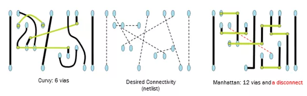
Curvy interconnects are able to reduce via count up to 50%, reducing die size and cost while improving yield. Source: Steve Teig, Perceive
Smith: Which areas in the design flow will need to change to accommodate curvy design?
Fujimura: To support curvy designs, changes will need to be made in physical design (place and route), extraction, design rule checking (DRC), and mask rule checking (MRC) tools. Some believe DRC and MRC will become easier with curvy design. Manufacturable curvy targets only need to be checked for manufacturability directly rather than guessing what the shape would become when manufactured.
For example, the design rules today need to be very complicated to describe the distance between two square vias placed kitty-corner opposite of each other. This is because the rules have to embed how the vias would actually end up being manufactured as circles. Manufacturable curvy targets would describe them as the circles that can be manufactured. So maximum curvature, minimum size, and minimum spacing would suffice to describe the geometric requirements on the shapes.
Smith: Sounds like an improvement but a big challenge?
 Fujimura: It’s definitely not happening overnight, that’s for sure. The possibility that EDA can enable a node’s worth of improvement is an exciting opportunity. We are in an era where 193 dry needs to try to go a node smaller, 193i needs to do as much as possible to alleviate the load on expensive EUV manufacturing, and .33 EUV needs to improve resolution to help reduce the number of layers requiring high-N/A EUV.
I’m hoping that the EDA community picks up on this. Curvy design wasn’t manufacturable six years ago. So, there’s been no reason to work on it until now. With GPU acceleration enabling the computing capabilities needed to support curvy design and manufacturing, the intersection of supply and demand of curvy design seems to be coming sooner rather than later.
About Aki Fujimura
Aki Fujimura is the Chairman and CEO of D2S, Inc. Previously, Fujimura served as CTO at Cadence Design Systems and returned to Cadence for the second time through the acquisition of Simplex Solutions where he was President/COO and inside board member. He was also an inside board member and VP at Pure Software. Simplex and Pure both went public during his tenure. Fujimura was a founding member of Tangent Systems, subsequently acquired by Cadence Design Systems. He was a board member of HLDS, RTime, Bristol, S7, and Coverity, Inc., all of which were successfully acquired. Fujimura received Bachelor of Science and Master of Science degrees in Electrical Engineering from MIT.
Robert (Bob) Smith is Executive Director of the ESD Alliance, a SEMI Technology Community.


