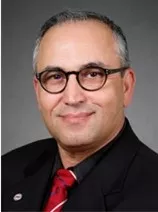
Silvaco is a well-established global technology provider of Technology Computer-Aided Design (TCAD), semiconductor intellectual property (IP) and electronic design automation (EDA) solutions to the semiconductor, photonics, and electronics industries. I recently spoke with Babak A. Taheri, Ph.D., the CEO of Silvaco, about the challenges of tuning and optimizing semiconductor manufacturing processes and how AI might be applied to reduce time and costs. Silvaco is a member of the ESD Alliance, a SEMI Technology Community.
Smith: What are the usual steps that fabs currently undertake to optimize their processes?
Taheri: It is usually achieved through trial and error. Process and fab engineers create and set up DoEs (design of experiments) that are realized in silicon. The resulting wafers are then analyzed to understand whether the process is meeting the desired targets. Some steps are automated, but the industry is still a long way from full automation of process optimization.
 One common way to evaluate process capability and performance is by gathering statistical measurements such as CpK and Cp. CpK is often called the process performance or capability measurement, while Cp is a simpler indicator that is usually called the process potential index. Engineers adjust process parameters to achieve the desired levels of Cp and CpK.
Current methodologies rely on performing multiple iterations using statistical data gleaned from physical wafers. Iterative process tuning can take weeks or months of experimentation to reach the desired result, which is costly.
Smith: Is there a way AI could play a role in automating fab process tuning?
Taheri: Yes, AI and machine learning (ML) can help reduce both fab tuning cycle times and the costs associated with having to fabricate multiple DoE runs. Both technologies achieve this by providing accurate models much faster than possible with the current trial and error approach.
This becomes even more important when considering that no two fab lines are identical. Even if the target process is the same, variations in the manufacturing equipment and their configurations mean that each line needs to be tuned independently. AI enables process optimization on an individual basis – per fab and line. In other words, the fab process parameters can be uniquely customized for each line.
AI can also help detect and prognosticate possible equipment failures and flag the need for preventive maintenance. The next generation of AI will be powered by physics and chemistry-based  solutions that tie to the physical fabrication technologies at the process, device, wafer, tool, and line levels.
Smith: There is a lot of discussion these days about the use of digital twins. Can the approach you are describing be likened to a digital twin?
Taheri: Yes, it fits the common definition of a digital twin, which is a comprehensive software-based model of a complex system. As I mentioned, AI and ML are ideally suited to rapidly building and improving models that mimic the behavior of complex physical systems. The digital twin is a crucial element of an AI-driven fab technology co-optimization flow (FTCOTM). It leverages software tools to drive the statistics based on the physical model considering the physics and chemistry of the process.
The models enable highly accurate process simulation from the outset, minimizing the number of DoEs without having to go through the time-consuming process of multiple trial and error calibrations of the process against the data gathered from the test wafers. Models developed using the digital twin closely match the analytical results that are captured from the process, DoEs and wafers, reducing the need for multiple wafer runs. This saves time and delivers significant cost savings.
Smith: Can the AI approach eliminate the need to run experiments in silicon?
Taheri: Using AI for FTCO can reduce the number of experiments required using actual silicon but cannot eliminate the need. The initial models require a starting point based on actual data from the physical devices and wafers. Once the models are refined by AI and ML, they can reduce the need for trial-and-error fab runs. As the models are optimized, feeding process data into them also reveals deviations that can trigger the need to service equipment before the process either drifts out of spec or even fails.
Smith: Using this approach, how do you know when are you done and have created a model that accurately represents the desired optimization for a particular process?
 Taheri: When the AI-based model closely aligns with actual measured data coming off the fab line, you have reached the point of having a good model. This is when we can call it the digital twin. Our approach applies physics and chemistry to model the process and the device characteristics on the wafer and in the fab. We often refer to this approach as physics/chemistry-based AI-driven modeling and optimization (PCAIOTM).
Smith: Has the AI-approach you are advocating been tested in real world conditions? If so, have the results met your expectations?
Taheri: All I can say right now is that we have been working closely with a major semiconductor provider to apply this methodology in a production flow. Early results from validating the flow are very encouraging.
Smith: How long do you think it will take the semiconductor industry to start implementing a process optimization flow that leverages AI? Is it already happening or is it further out in the future?
Taheri: AI adoption in the fab industry is already underway, as evidenced by our engagement with a leader in this space. We anticipate that more foundries will adopt similar AI-based methodologies to remain competitive.
About Dr. Taheri
 Babak A. Taheri, Ph.D., is CEO of Silvaco and a member of the company’s board of directors. Before rising to CEO, he served as Silvaco’s Chief Technology Officer and Executive Vice President of Products. Prior to joining Silvaco, Dr. Taheri served as CEO and President of Integrated Biosensing Technologies (IBT), an advisory and consulting firm. Dr. Taheri received a B.S. in engineering from San Francisco State University, an M.S. in electrical engineering from San Jose State University and a Ph.D. in biomedical engineering from the University of California, Davis.
Robert (Bob) Smith is executive director of the ESD Alliance, a SEMI Technology Community.