Charles Shi, Principal and Senior Analyst at Needham & Company, LLC., remains upbeat about the EDA, IP and services business, or what SEMI refers to as the electronic system design (ESD) ecosystem. I recently spoke with Shi about his talk Looking Forward to the New Chip Cycle during the opening of the 2023 Design Automation Conference, collocated in July with SEMICON West in San Francisco. Following are excerpts from our conversation.
Smith: You talked about how electronic design automation (EDA) has historically been cycle-proof, whereas the semiconductor industry goes through “boom and bust” cycles. Why the difference? Why doesn’t EDA also go through similar cycles?
Shi: It’s because EDA revenue comes from the R&D expense of the semiconductor industry. Imagine a fabless semiconductor company going into a downturn. The company will cut back wafer orders to foundries to get inventory and cost of goods sold (COGS) under control. It will reduce marketing dollars, lay off salespeople, and limit employee travel to cut back on selling, general and administrative (SG&A) expenses.
 It is unlikely that the company will lay off R&D engineers, especially chip design engineers, and instead will ask them to continue working as usual. Why? Because a chip design project usually lasts three years, but semiconductor downturns typically last for about a year. Cutting back R&D in a downturn means when the market comes back, the company will not have a competitive product to sell, and will lose market share to those who did not cut back R&D. This is fundamentally why EDA is cycle proof. I know there was skepticism about this thesis in 2022, but the strong results from Cadence and Synopsys prove that the thesis is largely correct.
Smith: You noted that Capital Expenditure (CapEx) in Wafer Fab Equipment (WFE) is falling. With all of the new fabs being proposed (or underway) in the U.S., when do you expect CapEx for WFE to grow again? Can we expect a big growth spurt given the number of new fabs coming online?
Shi: WFE will certainly grow again out of this downturn. The debate is not if, but when. If it doesn’t recover in 2024, it will certainly recover in 2025. However, semiconductor manufacturing is a fixed cost business. Other than chipmakers in China where CapEx is not quite funded by operating cash flows, most non-Chinese chipmakers will want to closely match supply to the demand. I do not believe that the new fabs in the U.S. being built by Intel, Samsung and TSMC are going to be built without demand. These are public companies that need to fulfill their fiduciary duties to shareholders and therefore cannot defy the gravity of economics.
We heard news that TSMC is delaying the production of its Arizona fab. There are many reasons to blame, but I think the fundamental reason is that we are still in a downturn. Without demand, TSMC will not and should not prematurely turn on the new capacity in Arizona. What this means is that I do not expect a growth spurt of WFE just because of the current push to build more fabs in the U.S. The growth spurt of global semiconductor demand will lead to a growth spurt for WFE.
Smith: Why is it that R&D spending in the semiconductor industry (not including memory) runs well below the R&D spending in EDA companies, for example 15% or less in semiconductor vs. more than 35% in EDA?. Is this the difference between developing software versus actually producing devices through a manufacturing process?
Shi: Yes, chip companies are hardware businesses and the model is different. When they budget their R&D expenses, they can only allocate money out of gross profits, which often are around 40-50% of the top line revenue. Even if they allocate 35% of their gross profits for R&D, that would only account for 15% of their revenue. However, for EDA companies, whose gross profits are often 80% of their revenue, they have a bigger pool of money, relatively speaking, to tap into for their R&D budgets.
 If they allocate 40% of their gross profits to R&D, it will translate to 30% of revenue. This is just simple math, but it tells you how powerful the EDA business model is. It is the very rare new economy business within the old economy sector of semiconductors. As such, the financial market values Cadence and Synopsys with a premium multiple when compared to traditional semiconductor stocks.
Smith: You had several slides that contrasted different semiconductor companies on financial metrics where you identified a leader and those who are trying to catch the leader (the chasers). Do you think the chasers have a chance to catch or overtake the leader?
Shi: I think the chances are very slim. Fundamentally, chipmaking is a capital-intensive business. The best analogy to this is utility companies. Ever wondered why there is only one utility company in most regions in the U.S.? This is because building power grids requires heavy capital investment.
The best way to make sure everyone gets cheap electricity is not to introduce a second utility provider, which would spend the same amount of money to build a redundant power grid. The best way is to only allow one utility company to build the power grid and, at the same time, make sure it does not abuse its market power.
With advanced semiconductor nodes getting exponentially more expensive to build, and in order to ensure the global tech industry can get cheap advanced semiconductors, the answer, in my opinion, is to allow TSMC, the leader, to thrive. Of course, it can’t abuse its market power, and this is where governments should play a larger role. The answer is not to create one or two TSMC clones. It will not work, in my humble opinion.
Smith: Everyone is talking about chiplets these days. How far away do you think we are from having chiplet design (whether.2.5D or 3D) become mainstream? What are the missing ingredients on the design side that will be needed to move chiplet-based design into the mainstream?
Shi: We are already in the chiplet era. There are chiplets in consumer devices today such as PCs, thanks to AMD’s chiplet-based CPU designs. We heard there will be chiplets in smartphones in about two or three years too, according to supply chain data. I expect that in the second half of this decade, chiplets will become mainstream in PCs and smartphones.
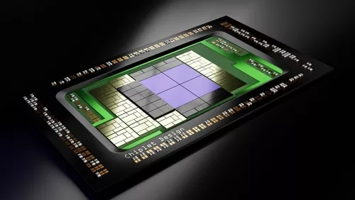 The missing ingredient, in my opinion, is the design enablement. Today, chiplets are mostly designed in silos by a handful of companies. There is not quite a robust open ecosystem there. For example, I believe AMD keeps its secret sauce of chiplet designs to itself. I think when foundries like TSMC come up with a 3D IC reference flow that is as robust as TSMC’s famed foundry reference flow and can be relied upon by chip designers who are not AMD or Apple, then we can say the ecosystem is established. Of course, building up a 3D IC reference flow requires close collaboration between foundries, EDA, IP and other ecosystem players. This takes time, but we are getting there.
Smith: Smith: Your slide (Foundry, EDA and IP as enablers of AI) shows the symbiotic relationships between the players in design and manufacturing. EDA suppliers and foundries are locked in a relationship where both are highly dependent on each other. Do you expect this to continue? Is there any reason to think that a mega-foundry would emerge that also supported its own tool flow for use internally and by customers?
Shi: Yes, these symbiotic relationships will continue into the future. New processes bring new capabilities for chip designers, which can only be realized with more advanced EDA tools. However, as EDA tools are generally not specific to processes, I see both the EDA industry and foundry industry peacefully coexisting with each other and happily collaborating well into the future. In addition, developing software and developing process are very different businesses and require very different skillsets. Foundries are probably not equipped to do this.
 However, on the IP side, things may be slightly trickier. I want to bring this up, as leading EDA companies are also leading IP providers. You probably know that TSMC actually developed its own foundational IPs such as standard cell and memory compilers. Previously, TSMC relied on external IP vendors. I think the reason why TSMC actually gets into the IP space is that IP, especially physical IP, is closely tied to the manufacturing process that TSMC sees as its core competency, and exerting tight control on those foundational IP makes strategic sense.
By the way, TSMC gives away foundational IP for free (or actually includes the IP costs in TSMC’s wafer prices), which largely kill this part of the IP market. I think something similar will likely play out in the 3D IC-related foundational IP. I don’t think mega-foundries like TSMC will support their own EDA tools, but they will support their own IP for use when it is critical for foundries to exert control over what they see as their core competency.
About Charles Shi
Charles Shi joined Needham & Company in 2019. He became a research analyst in 2021 covering Semiconductors and Semicap Equipment. Prior to Needham, Shi spent six years at Applied Materials, where he started as a global product manager in the metal deposition products division, and later became a business development manager covering the division’s foundry accounts. Shi received a Ph.D. in materials science and engineering and an MBA from the University of California, Berkeley, and a bachelor’s degree from Tsinghua University.
Robert (Bob) Smith is executive director of the ESD Alliance, a SEMI Technology Community.