
Synopsys recently introduced its cloud solution offering bring your own cloud (BYOC) and software as a service (SaaS) deployment model.
I recently spoke with Vikram Bhatia, Director of the Synopsys Cloud Go-to-Market and Product Strategy, on leveraging a flexible, pay-per-use approach to fuel the next phase of semiconductor innovation.
Smith: Design tool users blend flows that use tools from multiple EDA vendors. How difficult will it be for them to move to a single-source model?
Bhatia: With growing compute requirements, semiconductor companies are constantly being tested to deliver both complex functionality and best performance very quickly. Irrespective of where the customer is in their cloud journey, designers need to drive greater productivity and efficiency for complex chip design flows. Many users have big teams managing these flows, and it’s not uncommon for them to use tools from different vendors. Whether customers want to manage their own cloud or use a SaaS strategy, both approaches must accommodate heterogeneous tool flows as efficiently as possible.
Smith: Making EDA tools available via the cloud on a pay-per-use basis has been discussed for years. What are the breakthroughs that have enabled it to finally become a reality?
 Bhatia: There have been several breakthroughs in cloud technology itself as well as in the mindset of how users think about the pay-per-use model and how EDA vendors think about it. From a technology perspective, cloud computing has been around for a while, but being able to scale pay-per-use for EDA workloads automatically has only become possible because of the tight integration with cloud providers.
For instance, our SaaS solution is tightly integrated with the Microsoft Azure cloud platform, and our BYOC solution is available with Microsoft Azure, Amazon Web Services, and Google Cloud Platform. That means if a customer wants to run a simple flow and only uses one EDA tool to run a hundred copies of that tool on day one and run another 10,000 copies of the tool the next day, the underlying proprietary metering technology makes that possible seamlessly.
With the pay-per-use approach, users are no longer constrained by having to decide up front on the number of licenses for each tool and when it will be needed. A pay-per-use model flips that around, letting design needs dictate how and when designers use chip design and verification tools. As a result, chip designers have started to think differently. Teams can now decide how they want to run specific parts of the project without being limited to how many licenses they have and need to run. That’s a big breakthrough in user mindset.
Smith: What are the compelling economics of shifting to a SaaS-based cloud EDA methodology?
Bhatia: From an economics perspective, it is all about time-to-market. For most semiconductor companies, large or small, a significant part of their IT spending goes to the core of their business — designing a chip and getting it into manufacturing.
 Today, in on-prem environments especially, project cycles depend on how long it takes to run a particular workload. We’re now trying to approach that differently and make customers think about time-to-market and be able to differentiate themselves from competitors by coming to market first.
So, the economics of shifting methodologies are not tied to cost, which is important for customers trying to adjust to the pay-per-use mindset. In other words, by adopting this new methodology, customers can take advantage of a pricing and licensing approach that removes concern about cost increases and enables them to focus on their end goal: getting a quality product to market quickly.
A SaaS-based cloud EDA methodology should give teams a truly flexible model that accurately represents usage and aligns with solving today’s time-to-market needs.
Smith: Will this new usage-based cloud approach eventually replace the need for complex license management schemes?
Bhatia: We see a huge demand for technologies and business models from customers as they move to the cloud. We identified three key challenges that users currently face on-prem:
- Compute capacity: This is largely because there are more projects to do, increasingly complex chips to design, and less time to design them. The lead time to procure on-prem hardware is much longer as opposed to the cloud, where everything is available on-demand at scale.
- License management: Customers really want to spend their effort and time innovating and designing better chips than dealing with license server management. Almost every customer we've spoken to has told us about how they don't want to manage licenses but consider it a necessity to get the job done.
- Cutting edge compute: Access to the latest compute offerings, for example GPUs, is much easier, takes less time, and is less expensive when done on the cloud. The process to enable latest hardware is much harder on-prem, since customers need to plan ahead to commit large capital expenditures to procure these.
EDA tool flow and license management have remained a heavy lift. The ideal solution is to provide flexible on-demand tool access without the traditional license constraints. This helps to eliminate time spent forecasting needs and making compromises due to limited resources that may jeopardize design capabilities.
Smith: Can you offer more visibility on how usage is tracked? Is it a function of CPU capacity, CPU time, the tool being used and others? Does the number of users factor in?
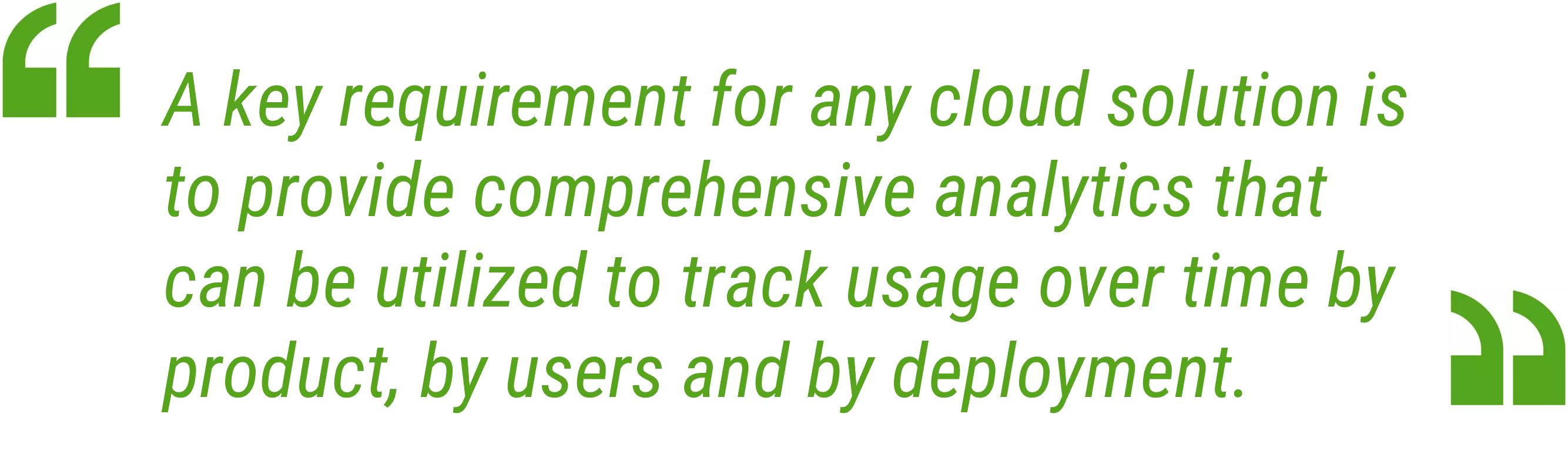
Bhatia: Usage is generally tracked via a unit of time such as by hour or minute. The number of users and projects is typically factored into the model as well. A key requirement for any cloud solution is to provide comprehensive analytics that can be utilized to track usage over time by product, by users and by deployment. Such an analysis capability makes it possible for a design team to leverage data and make better and quicker decisions. At Synopsys, we often refer to any tool, any scale, any time as our guiding principle in developing and evolving our solutions.
Smith: What models or variants are used in the industry today for pay-per-use and/or working via the cloud?
Bhatia: For on-prem, there are two types. The most common one is a traditional model that allows you to buy a certain number of licenses for a specific product for fixed terms such 3 years, 1 year or 6 months.
For those working on cloud, customers would take the licenses provided on-prem and deploy them on the cloud. The end user manages the entire process and must decide how many licenses need to be used and when they are required. With a cloud-based SaaS model in the equation, there isn’t a need to decide how much time or licenses needs to be allocated to a project.
One of the biggest advantages that the cloud provides for chip design is the virtually unlimited and advanced compute resources that deliver the capacity that designers need. Based on actual usage, teams can determine what decisions can be made better. For instance, if a 1,000-core cluster at a scale X took five hours to run, teams can use this information to decide whether there was scope for the project to run overnight, at a smaller scale, or use a bigger core count to complete the job faster.
Smith: How long do you think it will take the industry to move to a point where the majority of design teams are working in the cloud and using the pay-per-usage model?
 Bhatia: The success of the cloud model will largely depend on whether cloud and software vendors can continue to provide an excellent user experience and an application interface that is friendly and intuitive. Users shouldn’t feel threatened by an interface and must be able to easily grasp what the platform does after using it once, so that they can focus on the real job — designing a quality chip. As long as the user experience is seamless, the adoption will be faster. Compared to on-prem, there’s an immense value add from user interfaces in the cloud. This enables teams to make better decisions week after week — something that hasn’t been available until now.
With the pay-per-use model, users don’t need to quantify licenses and build the infrastructure up front. Instead, they can start small and test it out for a short period of time. Since all the features are on-demand, they can choose to grow their usage to make the most of their experience or choose to walk away. This can’t be done on-prem, so ultimately, it’s the user experience and supporting analytics that will determine the pace of cloud adoption for EDA.
EDA on the cloud continues to be a journey, one that is only getting more exciting. With the pace at which the semiconductor industry is moving, chip and system design will never be the same; that’s going to be a welcome transformation.
About Vikram Bhatia
 Vikram Bhatia is head of Cloud Go-to-Market (GTM) & Product Strategy at Synopsys. Before joining Synopsys, Vikram served in a variety of roles at companies including NetApp (VP of Cloud GTM Strategy and Business Operations), Oracle (director of Sales Strategy & Business Development for Oracle Cloud), and Microsoft (Director, Microsoft Azure). He has a bachelor’s of technology degree from the Indian Institute of Technology Kanpur, a master’s of science degree from the Colorado School of Mines, and an MBA from the Indian School of Business.