downloadGroupGroupnoun_press release_995423_000000 copyGroupnoun_Feed_96767_000000Group 19noun_pictures_1817522_000000Member company iconResource item iconStore item iconGroup 19Group 19noun_Photo_2085192_000000 Copynoun_presentation_2096081_000000Group 19Group Copy 7noun_webinar_692730_000000Path
Skip to main content

Methodics by Perforce Surveys Semiconductor Design Professionals on Product Lifecycle Management

Product lifecycle management is a well-adopted methodology used in mechanical design. Until recently, it was not widely used in the semiconductor industry. That all changed when Methodics created intellectual property lifecycle management for tracking and analysis of semiconductor IP and design.

Pre-Silicon Verification – The Newest Approach to Accelerating Time-to-Market of Advanced Computing Capabilities

“Virtual platform environments that combine the verification capabilities of emulation with the pre-silicon functionality insights available through verification intellectual property (VIP) are an increasingly popular way to get designs verified ahead of the curve of new standards,” Browy says.

IC Design Crashes Into the 3D Wall: Multiphysics Platforms Ride to the Rescue

Three-dimensional integrated circuits (3D-ICs) are revolutionizing the semiconductor industry. Manufactured by stacking and interconnecting dies so they perform as a single device, 3D-ICs deliver more capabilities by offering higher performance and bandwidth — while also reducing power consumption,...

For Moore’s Law to Live, SoCs Must Die

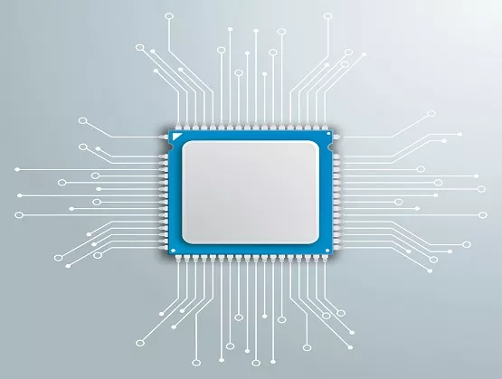
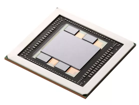
Throughout the current millennium, System-on-Chip (SoC) has been the gold standard for optimizing performance and cost of complete electronic systems. By incorporating practically all the phone’s digital plus analog capabilities onto a single, giant chip, the mobile phone processor serves as a...

Taking Atoms to Systems in Next-Generation SoC Designs

New system-on-chip (SoC) devices are driving new memory architectures and photonic interfaces, while specialized new intellectual property (IP) requires analysis down to the nanometer and atomic levels because of single nanometer process nodes. According to Babak Taheri, CTO and EVP of products at...

3D Heterogeneous Integration Drives Demand for New Materials and Integration Solutions

SEMI met with Gerald Beyer, program manager at imec, to discuss the co-existence of various 3D interconnect technologies and their need for new materials and integration solutions. The two talked in the runup to his presentation at the Advanced Packaging...