
S2C is an ESD Alliance member well situated in the field programmable gate array prototyping space with solutions Paving the way to digital innovation. Founded in 2004, S2C’s worldwide customer base uses its desktop and enterprise field programmable gate array (FPGA) prototyping tools to verify system on chip (SoC) and application-specific integrated circuit (ASIC) designs will work as intended.
I recently spoke with Ying Chen, S2C Vice President Marketing and International Sales, about trends and new applications in semiconductor design hardware verification and system validation.
Smith: What trends are you seeing in the FPGA prototyping market?
Chen: Users we talk with cite the need for an electronic design automation (EDA) cloud solution. The use of artificial intelligence and machine learning (AI/ML) in EDA and FPGA prototyping also comes up often in our discussions, as does growing demand for FPGA prototyping.
Smith: Do any of these trends surprise you?
Chen: No, they are based on real market demands. We anticipated these growth drivers and are prepared to support them.
 Big and small companies alike need EDA cloud computing as they look to take advantage of the efficiencies of cloud-based services. Big companies benefit by having multi-site collaboration over the cloud. Small companies benefit by reducing spending through a pay-for-use model.
Cloud-based solutions that leverage talent from remote locations are needed more than before to help companies cope with the current labor shortages because of COVID and the Great Resignation. Specifically, FPGA prototyping can benefit via a cloud deployment to ensure verifications are completed and repeated in the same environment.
The concern for security and the trust factor is still an issue and that takes time to overcome. Companies like S2C offer prototyping cloud services and cloud management packages for users who want to deploy their prototyping system in their own cloud.
The use of AI/ML is a critical aspect of FPGA prototyping for partitioning. An optimal partitioning strategy increases system performance and saves compile time. AI/ML can make sense of patterns to provide guidance for the partitioning topology and strategy.
 Demand is increasing for FPGA prototyping, a result of more SoC designs and SoC firmware/applications often tightly coupled in an SoC design. Companies can save six to nine months of time in the SoC design cycle if software development/verification is done on an FPGA prototype as opposed to having to wait for first silicon.
We also see value-conscious users choosing FPGA prototyping over emulation. Enterprise-class FPGA prototyping solutions can scale to emulation capacity while achieving performance five to 20 times faster than emulation and at a lower cost.
Smith: What are the differences between FPGA prototyping and emulation? What are the primary benefits of choosing FPGA prototyping as a verification solution over other solutions?
Chen: The spider chart below compares FPGA prototyping versus emulation. In short, FPGA prototyping is five to 100 times faster (or five to 20 times if partitioned) than emulation. The increased performance makes it feasible for SoC software/applications to be co-developed/verified, shortening the design cycle by six to nine months. The high performance also makes it possible for the device under test to interact with real-world data to catch real-world bugs. FPGA prototyping is a lower cost option than emulation.
Generally speaking, emulation is hardware-accelerated simulation. It provides high capacity and full visibility for trading off performance and cost. A well-funded design team may have an emulator or two to catch 90% of the hardware bugs. FPGA prototyping is used for in-circuit testing to catch the last 10% of hardware bugs and for software co-development/verification.
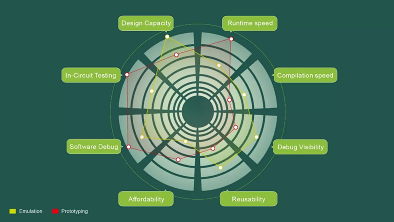
FPGA prototyping and emulation offer specific uses and benefits. Source: S2C
Smith: What new chip applications are you seeing?
Chen: Many different requirements from multiple market segments. The applications range from AI, graphics processing units (GPUs) and automotive to 5G/6G, storage and Internet of Things (IoT).
Smith: Do you see the shift-left methodology being widely adopted by verification engineers?
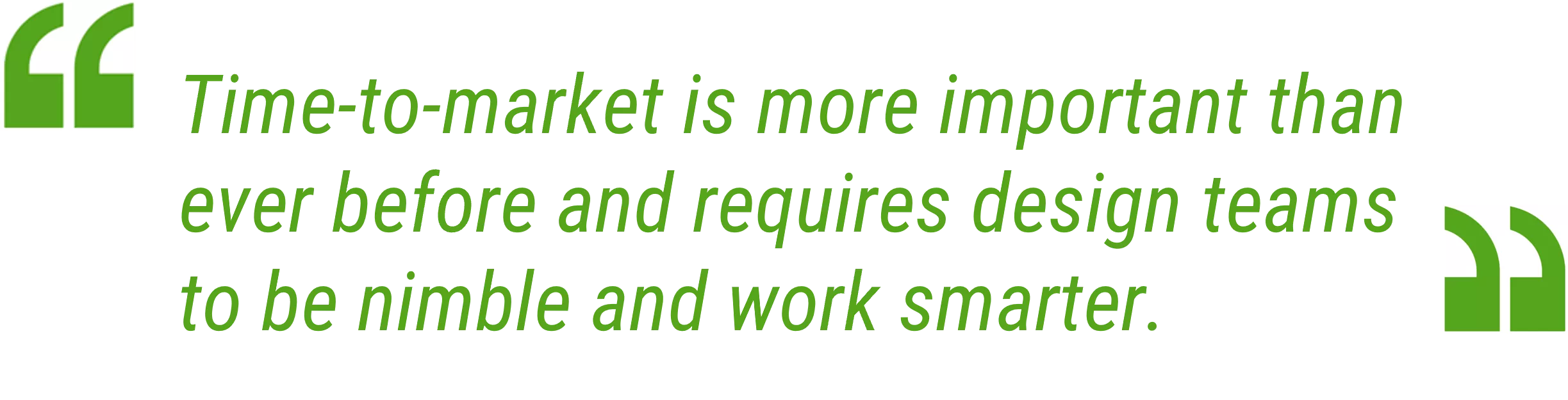
Chen: Yes, many of our customers are adopting FPGA prototyping because of the shift-left methodology that pushes verification earlier in the design cycle. Time-to-market is more important than ever before and requires design teams to be nimble and work smarter.
Smith: What new challenges are confronting verification engineers?
Chen: Many of the verification challenges are not new, just more pronounced. Time to market and the shortened design cycle always top the list. The shortage of verification engineers is getting worse.
Smith: Anecdotal signs in the chip design and verification space point to more software developers than hardware designers. Are you seeing that?
Chin: Yes. S2C, for example, has high-volume customers using FPGA prototyping systems in 20- to 80-unit quantities, not for capacity aggregation but for software co-development/verifications.
About Ying Chen
Ying Jen Chen is Vice President of Marketing and International Sales at S2C Limited. He is a dynamic technologist with more than 23 years of technical and business experience in the digital IC industry, including 20 years focused on the FPGA market. Prior to S2C, he was the head of APAC marketing at Lattice Semiconductor. Chen also held sales management and technical roles during his 15-year tenure at Altera in the U.S. and Taiwan. Chen received his bachelor’s degrees in Electrical Engineering and Computer Science (EECS) and Materials Sciences & Engineering from University of California, Berkeley.
Robert (Bob) Smith is executive director of the ESD Alliance, a SEMI Technology Community.